

SGS Thomson Microelectronics STGD7NB120S-1 Datasheet
TYPE V
CES
V
CE(sat)
STGD7NB120S-1 1200 V < 2.1 V 7 A
■ HIGHINPUTIMPEDANCE
(VOLTAGEDRIVEN)
■ VERYLOW ON-VOLTAGEDROP (V
■ HIGHCURRENT CAPABILITY
■ OFFLOSSES INCLUDE TAIL CURRENT
cesat
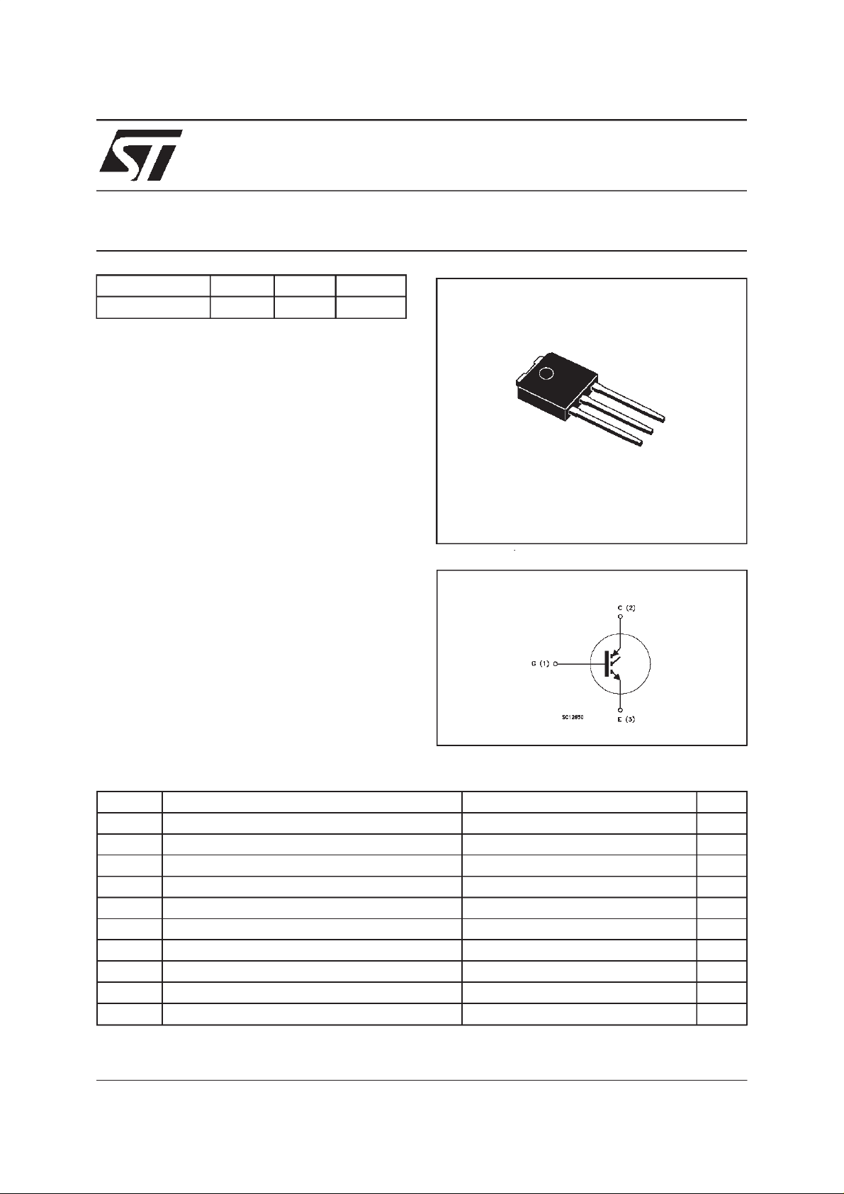
STGD7NB120S-1
N-CHANNEL 7A - 1200V IPAK
Power MESH IGBT
PRELIMINARY DATA
I
C
)
DESCRIPTION
Using the latest high voltage technology based
on a patented strip layout, STMicroelectronics
has designed an advanced family of IGBTs, the
PowerMESH IGBTs, with outstanding
perfomances. The suffix ”S” identifies a family
optimized to achieve minimum on-voltage drop
IPAK
TO-251
(Suffix”-1”)
3
2
1
for low frequencyapplications(<1kHz).
APPLICATIONS
■ LIGHT DIMMER
■ INRUSHCURRENT LIMITATION
■ MOTORCONTROL
INTERNAL SCHEMATIC DIAGRAM
ABSOLUTE MAXIMUM RATINGS
Symb o l Parameter Value Unit
V
V
V
I
CM
P
T
(•) Pulse width limited by safe operating area
Collect o r -Em i t t er Voltage ( VGS= 0) 1200 V
CES
Reverse Battery Protection 20 V
ECR
Gate-Emitter Voltage
GE
I
Collect o r Curr ent ( con t inuous) at Tc=25oC10A
C
I
Collect o r Curr ent ( con t inuous) at Tc= 100oC7A
C
20 V
±
(•) Collector Curr ent (pulsed) 20 A
Tot al Di s si pat ion at Tc=25oC55W
tot
Derat ing Factor 0.4 W/
Sto rage Tem perature -65 to 15 0
stg
T
Max. Operat ing Junc tion Tem per ature 150
j
o
C
o
C
o
C
April 2000
1/6
STGD7NB120S-1
THERMAL DATA
R
thj-case
R
thj-amb
R
thc-sink
Ther mal Resistanc e Junct ion-case Max
Ther mal Resistanc e Junct ion-ambient Max
Ther mal Resistanc e Case-sink Ty p
2.27
100
1.5
o
C/W
o
C/W
o
C/W
ELECTRICAL CHARACTERISTICS
=25oC unless otherwisespecified)
(T
j
OFF
Symbol Parameter Test Conditions Min. Typ. Max. Unit
V
BR(CES)
Collector-Emitter
IC=250µAVGE= 0 1200 V
Break dow n Volt age
V
BR(ECR)
Emitter-Collector
IC = 10 mA VGE=0 20 V
Break dow n Volt age
I
I
CES
GES
Collect o r cut - off
=0)
(V
GE
Gat e- Em i t t er Lea k age
Current (V
CE
=0)
V
=MaxRating Tj=25oC
CE
=0.8MaxRating Tj= 125oC
V
CE
V
= ± 20 V VCE=0 ±100 nA
GE
250
1000
ON(∗)
Symbol Parameter Test Conditions Min. Typ. Max. Unit
V
GE(th)
Gate Threshold
VCE=VGEIC= 250 µ A35V
Voltage
V
V
CE(SAT)
Gat e Em it t er Volt age VCE=2.5V IC=2A Tj=25 ÷125oC6.5V
GE
Collector-Emitter
Sat urat ion Volt age
VGE=15V IC=3.5A
=15V IC=7A
V
GE
V
=15V IC=10A 1.7
GE
1.6
2.1
DYNAMIC
µ
µA
V
V
V
A
Symbol Parameter Test Conditions Min. Typ. Max. Unit
g
Forward
fs
VCE=25 V IC=7A 2.5 4.5 S
Tr ansc on duc tance
C
C
C
Input C apacitance
ies
Out put Capacitance
oes
Reverse Tr ansfer
res
VCE=25V f=1MHz VGE= 0 430
40
7
Capacit a nc e
Q
I
CL
Gat e Charge VCE= 960 V IC=7A VGE= 15 V 29 nC
G
Latc hing Curr ent V
=960V RG=1kΩ
clamp
= 150oC
T
j
10 A
SWITCHINGON
Symbol Parameter Test Conditions Min. Typ. Max. Unit
(di/dt)
2/6
t
d(on)
E
Delay Time
t
Rise Ti m e
r
Tur n-on Current Slope
on
Turn-on
on
Switching Losses
VCC= 960 V IC=7A
=15V RG=1KΩ
V
GE
VCC=960V IC=7A
=1KΩ VGE=15V
R
G
T
=125oC
j
570
270
800
3.2
pF
pF
pF
ns
ns
A/µs
mJ
 Loading...