

SGS Thomson Microelectronics STGB7NB60HDT4 Datasheet
STGB7NB60HD
N-CHANNEL 7A - 600V DPAK
PowerMESH IGBT
■
HIGH INPUT IMPEDANCE
(VOLTAGE DRIVEN)
■
LOW ON-VOLTAGE DROP (V
cesat
)
■
LOW GATE CHARGE
■
HIGH CURRENT CAPABILITY
■
VERY HIGH FREQUENCY OPERATION
■
OFF LOSSES INCLUDE TAIL CURRENT
■
CO-PACKAGED WITH TURBOSWITCH
ANTIPARALLEL DIODE
■
SURFACE-MOU NTING D2PAK (TO-263)
POWER PACKAGE IN TA PE & REEL
(SUFFIX "T4")
DESCRIPTION
Using the latest high voltage technology based
on a patented strip layout, STMicroelectronics
has designed an advanced family of IGBTs, the
PowerMESH IGBTs, with outstanding
perfomances. The suffix "H" identifies a family
optimized to achieve very low switching times for
high frequency applications (<120kHz).
APPLICATIONS
■
HIGH FREQUENCY MOTOR CONTROLS
■
SMPS AND PFC IN BOTH HARD SWITCH
AND RESONANT TOPOLOGIES
®
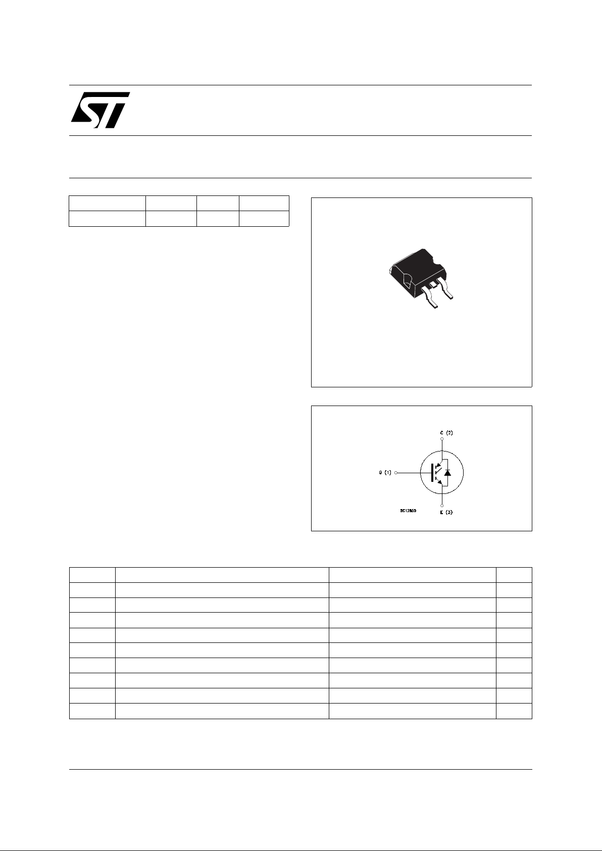
INTERNAL SCHEMATIC DIAGRAM
ABSOLUTE MAXIMUM RATINGS
Symbol Parameter Value Unit
V
CES
Collector-Emitter Voltage (VGS = 0) 600 V
V
GE
Gate-Emitter Voltage ± 20 V
I
C
Collector Current (continuous) at Tc = 25 oC14A
I
C
Collector Current (continuous) at Tc = 100 oC7A
I
CM
(•) Collector Current (pulsed) 56 A
P
tot
Total Dissipation at Tc = 25 oC80W
Derating Factor 0.64 W/
o
C
T
stg
Storage Temperature -65 to 150
o
C
T
j
Max. Operating Junction Temperature 150
o
C
(•) Pulse width limited by safe operating area
TYPE V
CES
V
CE(sat)
I
C
STGB7NB60HD 600 V < 2.8 V 7 A
June 1999
1
3
D2PAK
TO-263
(Suffix "T 4")
1/8
THERMAL DATA
R
thj-case
R
thj-amb
R
thc-sink
Thermal Resistance Junction-case Max
Thermal Resistance Junction-ambient Max
Thermal Resistance Case-sink Typ
1.56
62.5
0.5
o
C/W
o
C/W
o
C/W
ELECTRICAL CHARACTERISTICS
(T
j
= 25 oC unless otherwise specified)
OFF
Symbol Parameter Test Conditions Min. Typ. Max. Unit
V
BR(CES)
Collector-Emitter
Breakdown Voltage
IC = 250 µA V
GE
= 0 600 V
I
CES
Collector cut-off
(V
GE
= 0)
V
CE
= Max Rating Tj = 25 oC
V
CE
= Max Rating Tj = 125 oC
250
2000
µA
µA
I
GES
Gate-Emitter Leakage
Current (V
CE
= 0)
V
GE
= ± 20 V VCE = 0 ± 100 nA
ON (∗)
Symbol Parameter Test Conditions Min. Typ. Max. Unit
V
GE(th)
Gate Threshold
Voltage
V
CE
= VGE IC = 250 µA35V
V
CE(SAT)
Collector-Emitter
Saturation Voltage
VGE = 15 V IC = 7 A
V
GE
= 15 V IC = 7 A Tj = 125 oC
2.3
1.9
2.8 V
V
DYNAMIC
Symbol Parameter Test Conditions Min. Typ. Max. Unit
g
fs
Forward
Transconductance
VCE =25 V IC = 7 A 3.5 5 S
C
ies
C
oes
C
res
Input Capacitance
Output Capacitance
Reverse Transfer
Capacitance
V
CE
= 25 V f = 1 MHz V
GE
= 0 390
45
10
560
68
15
730
90
20
pF
pF
pF
Q
G
Q
GE
Q
GC
Total Gate Charge
Gate-Emitter Charge
Gate-Collector Charge
VCE = 480 V IC = 7 A VGE = 15 V 42
7.9
17.6
55 nC
nC
nC
I
CL
Latching Current V
clamp
= 480 V RG=10Ω
T
j
= 150 oC
28 A
SWITCHING ON
Symbol Parameter Test Conditions Min. Typ. M ax. Unit
t
d(on)
t
r
Delay Time
Rise Time
VCC = 480 V IC = 7 A
V
GE
= 15 V RG = 10Ω
15
48
ns
ns
(di/dt)
on
Eon(❍)
Turn-on Current Slope
Turn-on Switching
Losses
V
CC
= 480 V IC = 7 A
R
G
= 10 Ω VGE = 15 V
T
j
= 125 oC
160
185
A/µs
µJ
STGB7NB60HD
2/8
ELECTRICAL CHARACTERISTICS (continued)
SWITCHING OFF
Symbol Parameter Test Conditions Min. Typ. Max. Unit
t
c
tr(v
off
)
t
d
(off)
t
f
E
off
(**)
E
ts
(❍)
Cross-Over Time
Off Voltage Rise Time
Delay Time
Fall Time
Turn-off Switching Loss
Total Switching Loss
VCC = 480 V I
C
= 7 A
R
GE
= 10 Ω VGE = 15 V
85
20
75
70
85
235
ns
ns
ns
ns
µ
J
µ
J
t
c
tr(v
off
)
t
d
(off)
t
f
E
off
(**)
E
ts
(❍)
Cross-Over Time
Off Voltage Rise Time
Delay Time
Fall Time
Turn-off Switching Loss
Total Switching Loss
VCC = 480 V I
C
= 7 A
R
GE
= 10 Ω VGE = 15 V
T
j
= 125 oC
150
50
110
110
220
405
ns
ns
ns
ns
µ
J
µ
J
COLLECTOR-EMITTER DIODE
Symbol Parameter Test Conditions Min. Typ. Max. Unit
I
f
I
fm
Forward Current
Forward Current pulsed
7
56
A
A
V
f
Forward On-Voltage If = 7 A
I
f
= 7 A Tj = 125 oC
1.6
1.4
2.0 V
V
t
rr
Q
rr
I
rrm
Reverse Recovery Time
Reverse Recovery Charge
Reverse Recovery Current
If = 7 A VR=200 V
dI/dt = 100 A/µS T
j
= 125 oC
100
180
3.6
ns
nC
A
(•) Pulse width limited by max. junction temperature
(
❍
) Include recovery losses on the STTA506 freewheeling diode
(∗) Pulsed: Pulse duration = 300 µs, duty cycle 1.5 %
(**)Losses Include Also The Tail (Jedec Standardi zat io n)
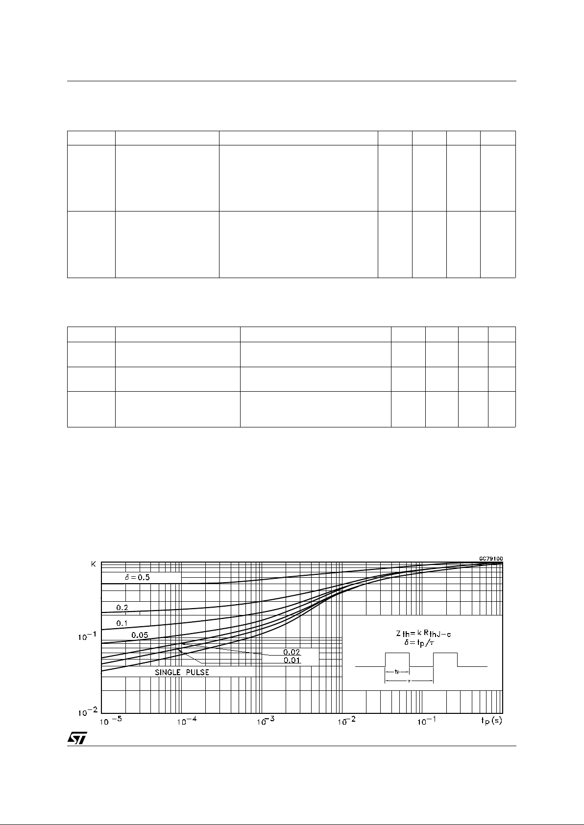
Thermal Impedance
STGB7NB60HD
3/8
 Loading...