

SGS Thomson Microelectronics STGB7NB40LZ Datasheet
STGB7NB40LZ
N-CHANNEL CLAMPED 14A - D2PAK
INTERNALLY CLAMPED PowerMESH™ IGBT
TYPE V
CES
V
CE(sat)
I
C
STGB7NB40LZ CLAMPED < 1.50 V14A
■ POLYSILICON GATE VOLTAGE DRIVEN
■ LOW THRESHOLD VOLTAGE
■ LOW ON-VOLTAGE DROP
■ LOW GATE CHARGE
■ HIGH CURRENT CAPABILITY
■ HIGH VOLTAGE CLAMPING FEATURE
DESCRIPTION
Using thelatest highvoltage t echnology based on a
patented strip layout, STMicroelectronics has
designed an advanced family of IG BTs, the
PowerMESH
™
IGBTs, with outstanding
performances. The built in collector-gate zener
exhibits a very precise active clamping while the
gate-emitter zener supplies an ESD protection.
APPLICATIONS
■ AUTOMOTIVE IGNITION
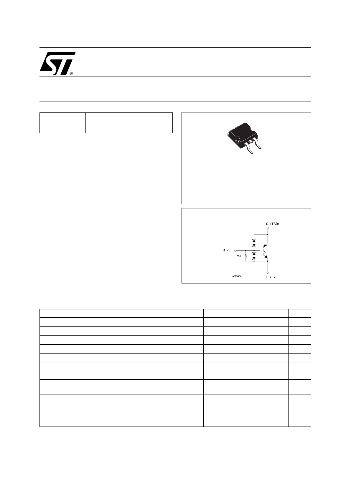
3
1
D2PAK
INTERNAL SCHEMATIC DIAGRAM
ABSOLUTE MAXIMUM RATINGS
Symbol Parameter Value Unit
V
V
V
P
E
CES
ECR
GE
I
C
R
G
TOT
E
CL
ECAV
T
stg
T
j
Collector-Emitter Voltage (VGS=0)
CLAMPED V
Reverse Battery Protection 20 V
Gate-Emitter Voltage CLAMPED V
Collector Current (continuous) at 100°C 14 A
Minimum External Gate Resistor 500 Ω
Total Dissipation at TC= 25°C
100 W
Derating Factor 0.66 W/°C
Single Pulse Collector to Emitter Avalanche Energy
=13A;Tj= 150°C (see fig.1-2)
I
C
Reverse Avalanche Energy
= 7 A ;f= 100 Hz ; Tc= 25°C
I
C
Storage Temperature
Operating Junction Temperature
130 mJ
10 mJ
–55 to 175 °C
1/8March 2003
STGB7NB40LZ
THERMAL DATA
Rthj-case Thermal Resistance Junction-case Max 1.5 °C/W
Rthj-amb Thermal Resistance Junction-ambient Max (free air) 62.5 °C/W
ELECTRICAL CHARACTERISTICS (T
= 25°C UNLESS OTHERWISE SPECIFIED)
CASE
OFF
Symbol Parameter Test Conditions Min. Typ. Max. Unit
BV
BV
(CES)
(ECS)
Collector-Emitter Clamped
Voltage
Emitter Collector Break-down
IC=10mA,VGE=0,
370 400 430 V
Tc= - 40°C to 150°C; RG=1KΩ
IEC= 75 mA, VGE=0, 20 27 V
Voltage
BV
GE
Gate Emitter Break-down
IG=±2mA 12 16 V
Voltage
I
CES
I
GES
Collector-Emitter Leakage
Current
Gate-Emitter Leakage
Current (V
CE
=0)
VGE=200V,VGE=0,RG=1KΩ
Tc=25°C
Tc=150°C
V
=±10V,VCE= 0 1000 µA
GE
25
250
ON (1)
Symbol Parameter Test Conditions Min. Typ. Max. Unit
V
GE(th)
V
CE(SAT)
R
GE
Gate Threshold Voltage VCE=VGE,IC= 1 mA, Tc=25°C
= 1 mA, Tc=150°C
Collector-Emitter Saturation
Voltage
V
CE=VGE,IC
VGE=4.5 V, IC=7A,Tj=25°C
V
=5.0 V, IC=14A,Tc=25°C
GE
Gate Emitter Resistance
1.2
0.75
1.3 1.50
10 20
2.2
1.8
1.9
30
DYNAMIC
Symbol Parameter Test Conditions Min. Typ. Max. Unit
V
C
ies
C
oes
C
res
Input Capacitance
Output Capacitance 80 pF
Reverse Transfer
Capacitance
Q
g
Gate Charge VCE=40V,IC=7A,
=25V,f=1MHz,VGE=0
CE
V
=5V
GE
910 pF
15 pF
22 nC
µA
µA
V
V
V
V
KΩ
SWITCHING ON
Symbol Parameter Test Conditions Min. Typ. Max. Unit
=14V,RG=1KΩ,
V
CE
RL=1Ω, VGE=5 V
VCE= 300 V, RG=1KΩ ,
R
=46Ω, VGE=5 V
L
0.9
4.5
4.4
3.6
2/8
t
d(on)
t
d(off)
Delay Time
t
r
Current Rise Time
Delay Time
t
f
Current Fall Time
µs
µs
µs
µs
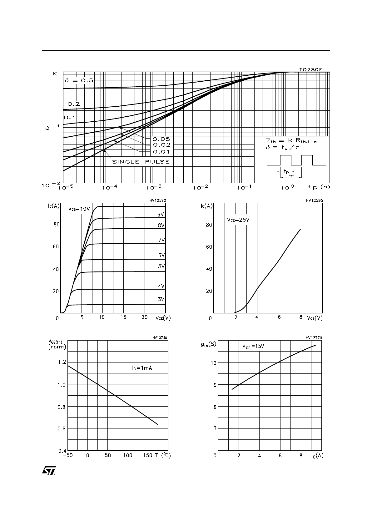
Thermal Imped ance
STGB7NB40LZ
Output Characteristics
Normalized Gate Threshold Voltage vs Temp. Transconductance
Transfer Characteristics
3/8
 Loading...