

SGS Thomson Microelectronics STGB3NB60SDT4 Datasheet
1/8November 2000
STGB3NB60SD
N-CHANNEL 3A - 600V D2PAK
Power MESH™ IGBT
■ HIGH INPUT IMPEDANCE
(VOLTAGE DRIVEN)
■ VERY LOW ON-VOLTAGE DROP (V
cesat
)
■ HIGH CURRENT CAPABILITY
■ OFF LOSSES INCLUDE TAIL CURRENT
■ INTEGRATED FREEWHEELING DIODE
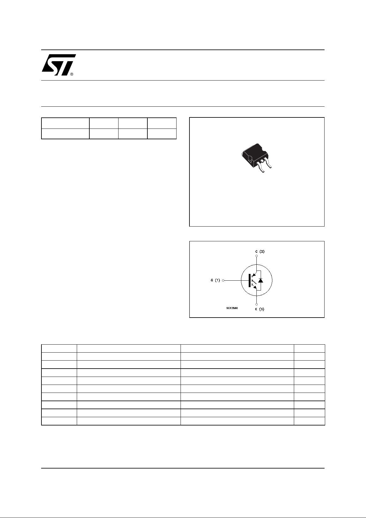
■ SURFACE-MOUNTING D
2
PAK (TO-263)
POWER PACKAGE IN TAPE & REEL
(SUFFIX “T4”)
DESCRIPTION
Using the latest high voltage technology based on a
patented strip layout, STMicroelectronics has designed
an advanced fa mily o f IGB Ts, the PowerMESH™ IGB Ts,
with outstanding pe rfomances . The suffix “S” identifi es a
family optimized to a chiev e minim um on -volta ge drop for
low frequency applications (<1kHz).
APPLICATIONS
■ GAS DISCHARGE LAMP
■ STATIC RELAYS
■ MOTOR CONTROL
TYPE
V
CES
V
CE(sat)
I
c
STGB3NB60SD 600 V <1.5 V 3 A
D2PAK
TO-263
(suffix“T4”)
1
3
ABSOLUTE MAXIMUM RATINGS
(•)Pulse w id th limited by s afe operating area.
Symbol Parameter Value Unit
V
CES
Collector-Emitter Voltage (VGS = 0) 600 V
V
GE
Gate-Emitter Voltag e ± 20 V
I
C
Collector Current (continuos) at Tc=25°C 6 A
I
C
Collector Current (continuos)at Tc=100°C 3 A
I
CM
(•) Collector Current (pulsed) 25 A
P
tot
Total Dissipation at Tc = 25°C 70 W
Derating Factor 0.46 W/°C
T
stg
Storage Temperature –60 to 175 °C
T
j
Max. Operating Junction Temperature 175 °C
INTERNAL SCHEMATIC DIAGRAM
STGB3NB60SD
2/8
THERMA L D ATA
ELECTRICAL CHARACTERISTICS (T
case
= 25 °C unless otherwise specified)
OFF
ON
(*)
DYNAMIC
SWITCHING ON
R
thj-case
Thermal Resistance Junction-case Max 2.14 °C/W
R
thj-amb
Thermal Resistance Junction-ambient Max 62.5 °C/W
R
thc-sink
Thermal Resistance Case-sink Typ 0.5 °C/W
Symbol Parameter Test Conditions Min. Typ. Max. Unit
V
BR(CES)
Collector-Emitter
Breakdown Voltage
ID = 250 µA VGE = 0 600
V
I
CES
Collector cut-off (VGE = 0) VCE = Max Rating Tj = 25 °C
V
CE
= Max Rating Tj = 125 °C
10
100
µA
µA
I
GSS
Gate-body Leakage
Current (V
DS
= 0)
V
GS
= ± 20V VCE = 0
±100 nA
Symbol Parameter Test Conditions Min. Typ. Max. Unit
V
GE(th)
Gate Threshold Voltage
V
CE
= VGE I
C
= 250 µA
2.5 5 V
V
CE(SAT)
Collector-Emitter Saturation
Voltage
V
GE
= 15 V IC = 1.5 A
V
GE
= 15 V IC = 3 A
V
GE
= 15 V ID = 3 A Tj = 125 °C
1
1.2
1.1
1.5
V
V
V
Symbol Parameter Test Conditions Min. Typ. Max. Unit
g
fs
Forward Transconductance VCE = 25 V IC = 3 A 1.7 2.5 S
C
ies
Input Capacitance VCE = 25V f = 1 MHz VGE = 0 255 330 pF
C
oes
Output Capacitance 30 40 pF
C
res
Reverse Transfer Capacitances
5.6 7 pF
Q
G
Total Gate Charge VCE=480V IC=3 A VGE=15 V 18 nC
Q
GE
Gate-Emitter Charge 5.4 nC
Q
GC
Gate-Collector Charge 5.5 nC
I
CL
Latching Current V
clamp
= 480 V RG = 1 K
Ω
T
j
=150 °C
12 A
Symbol Parameter Test Conditions Min. Typ. Max. Unit
t
d(on)
t
r
DelayTime
Rise Time
VCC = 480 V IC = 3 A
V
GE
= 15 V RG = 1 k
Ω
125
150
ns
ns
(di/dt)
on
E
on
Turn-on Current Slope
Turn-on Switching Losses
VCC = 480 V IC = 3 A
V
GE
= 15 V RG = 1 k
Ω
T
j
=125 °C
50
1100
A/µs
µ
J
3/8
STGB3NB60SD
SWITCHING OFF
COLLECTOR-EMITTER DIODE
(•)Pulse width li m i ted by max. junction temperature
(*)Pulsed: Pulse dur ation = 300 µs, duty cycle 1. 5 %.
(∗∗)Losses I nclude Also T he Tail (Jedec St andardization)
Symbol Parameter Test Conditions Min. Typ. Max. Unit
t
c
tr(
Voff
)
t
d(Voff
)
t
f
E
off(**
)
Cross-Over Time
Off Voltage Rise Time
Delay Time
Fall Time
Turn-off Switching Loss
V
CC
= 480 V IC = 3 A
R
GE
= 1 k
Ω
VGE = 15 V
1.8
1.0
3.4
0.72
1.15
µ
s
µ
s
µ
s
µ
s
mJ
t
c
tr(
Voff
)
t
d(Voff
)
t
f
E
off(**
)
Cross-Over Time
Off Voltage Rise Time
Delay Time
Fall Time
Turn-off Switching Loss
V
CC
= 480 V IC = 3 A
R
GE
= 1 k
Ω
VGE = 15 V
T
j
= 125 °C
2.8
1.45
3.6
1.2
1.8
µ
s
µ
s
µ
s
µ
s
mJ
Symbol Parameter Test Conditions Min. Typ. Max. Unit
I
f
I
fm
Forward Current
Forward Current pulsed
3
25
A
A
V
f
Forward On-Voltage
I
f
= 3 A
I
f
= 1 A
1.55
1.15
1.9 V
V
t
rr
Q
rr
I
rrm
Reverse Recovery Time
Reverse Recovery Charge
Reverse Recovery Current
If = 3 A VR = 200 V
di/dt = 100 A/µs T
j
= 125 °C
1700
4500
9.5
ns
nC
A
ELECTRICAL CHARACTERISTICS (continued)
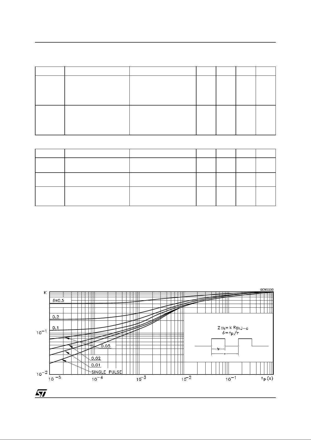
Thermal Impedance
 Loading...