

SGS Thomson Microelectronics STG3157CTR Datasheet
LOW VOLTAGE LOW ON RESISTANCE SPDT SWITCH
WITH BREAK BEFORE MAKE FEATURE
■ HIGH SPEED:
t
= 0.3ns (MAX.) at VCC=4.5V
PD
t
= 0.8ns (MAX.) at VCC=3.0V
PD
= 1.2ns (MAX.) at VCC=2.3V
t
PD
■ VERY LOW POWER DISSIPATION:
=1µA(MAX.) at TA=85°C
I
CC
■ LOW "ON" RESISTANCE V
=7Ω(MAX.TA=85°C) atVCC=4.5V
R
ON
R
=9Ω(MAX. TA=85°C) at VCC=3.0V
ON
■ WIDE OPERATING VOLTAGE RANGE:
V
(OPR) = 1.65V to 5.5V SI NGLE SU PPLY
CC
■ TTL THRESOLD ON CONTROL INPUT at
V
= 2.7 to 3.6V
CC
■ PIN AND FUNCTION COMPATIBLE WITH
74 SERIES 3157
■ LATCH-UP PE RFORMANCE EXCEEDS
300mA (JESD 17)
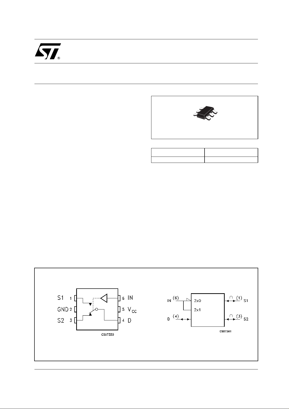
DESCRIPTION
The STG3157 is an high-speed spdt CMOS
ANALOG S.P.D.T. (Single Pole Dual Throw)
SWITCH or 2:1 Multiplexer/Demultiplexer Bus
Switch fabricated in silicon gate C
tecnology. It designed to operate from 1.65V to
5.5V, making this device ideal for portable
applications.
It offers very low ON-Resistance (<9
V
=3.0V. The IN input is provided to control the
CC
S.P.D.T. switch, it’s compatible with standard
IN
=0V:
2
MOS
Ω)at
STG3157
SOT323-6L
ORDER CODES
PACKAGE T & R
SOT323-6L STG3157CTR
CMOS output . The switch S1 is ON (it is
connected to c ommon Port D) w hen the IN input is
held high and OFF (high impedance state exists
between the two ports) wh en IN is held low; the
switch S2 is ON (it is connected to common Port
D) when the IN input is held low and OFF (high
impedance state exist s between the two ports)
when IN is held high. Additional key faetures are
fast switching speed, Break Before Make Delay
Time and Very Low Power Consumption. All
inputs and output are equipped with protection
circuits against static discharge, giving them ESD
immunity and transient exces s voltage.
It’s available in the commercial temperature range
in smallest s ix lead smd package on the market.
PIN CONNECTION AND IEC LOGIC SYMB OLS
1/10September 2002
STG3157
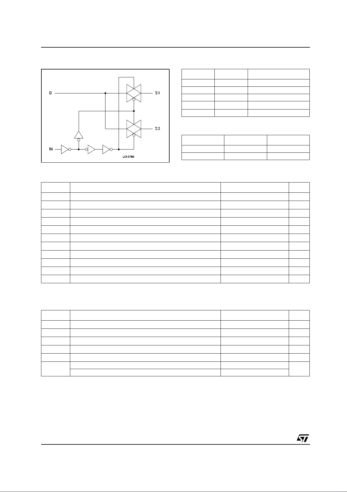
INPUT EQUIVALENT CIRCUIT PIN DESCRIPTION
PIN No SYMBOL NAME AND FUNCTION
1, 3 S1, S2 Independent Channel
4 D Common Channel
6 IN Control
5
2 GND Ground (0V)
TRUTH TABLE
IN SWITCH S1 SWITCH S2
H ON OFF(*)
L OFF(*) ON
*) High Impedance
ABSOLUTE MAXIMUM RATINGS
Symbol Parameter Value Unit
V
V
V
V
I
IKC
I
I
OK
I
or I
I
CC
T
T
Absolute Maximum Ratings are those values beyond which damage to the device may occour. Functional operation under these condition is
not implied
Supply Voltage
CC
DC Input Voltage -0.5 to VCC+ 0.5
I
DC Control Input Voltage
IC
DC Output Voltage -0.5 to VCC+ 0.5
O
DC Input Diode Current on control pin (VIN<0V)
DC Input Diode Current (VIN< 0V)
IK
DC Output Diode Current
DC Output Current
O
DC VCCor Ground Current
GND
Storage Temperature
stg
Lead Temperature (10 sec)
L
V
CC
Positive Supply Voltage
-0.5 to +7.0 V
-0.5 to Vcc + 0.5 V
± 50 mA
± 50 mA
± 20 mA
+ 128 mA
± 100 mA
-65 to +150 °C
300 °C
V
V
RECOMMENDED OPERATING CONDITIONS
Symbol Parameter Value Unit
V
V
V
V
T
dt/dv
1) Truth Table guaranteed: 1.2V to 6.0V
2/10
Supply Voltage (note 1)
CC
Input Voltage 0 to V
I
Control Input Voltage
IC
Output Voltage 0 to V
O
Operating Temperature
op
Input Rise and Fall Time Control Input for Vcc= 2.3V - 3.6V 0 to 10
Input Rise and Fall Time Control Input for Vcc= 4.5V - 5.5V 0 to 5
1.65 to 5.5 V
CC
0 to 5.5 V
CC
-55 to 125 °C
V
V
ns/V
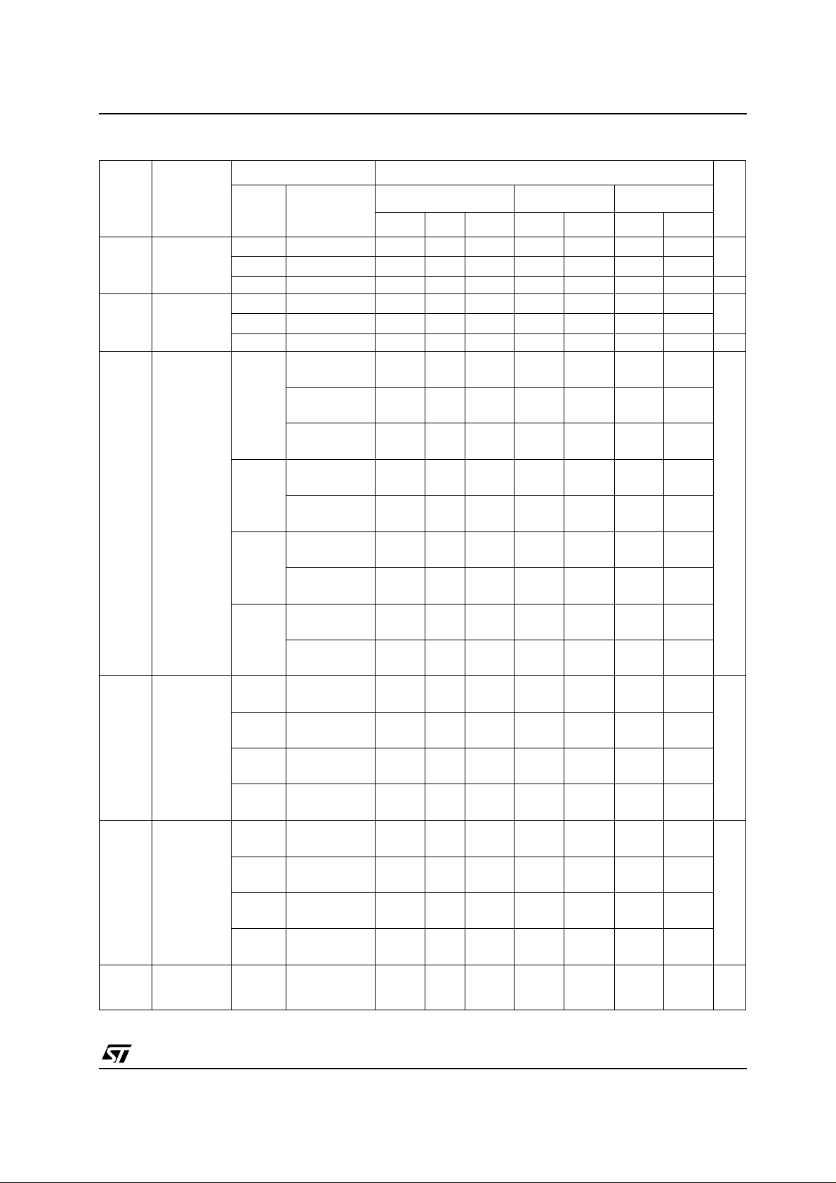
DC S PEC IFICATIONS
Symbol Parameter
V
High Level
IH
Input Voltage
V
Low Level
IL
Input Voltage
R
Switch ON
ON
Resistance
∆R
R
FLAT
I
OFF
ON
ON
Resistance
Match
between
channels
ON
Resistance
FLATNESS
OFF State
Leakage
Current
Test Condition Value
=25°C
T
V
CC
(V)
1.65-1.95 0.75V
2.3-5.5
2.7-3.6
1.65-1.95 0.25V
2.3-5.5
2.7-3.6
4.5 VS=0V
I
=30mA
S
=2.4V
V
S
I
=30mA
S
= 4.5V
V
S
I
=30mA
S
I
=24mA
S
V
I
=24mA
S
I
S
V
S
I
S
I
S
V
=1.65V
S
I
S
=3.15V
S
=30mA
I
S
S
I
=24mA
S
S
I
S
=1.15V
S
I
S
=0V
S
=3V
S
=0V
S
=8mA
=2.3V
=8mA
=0V
S
=4mA
=4mA
=2.1V
=1.6V
=8mA
=4mA
CC
3.0 V
2.3 V
1.65 V
4.5 V
3.0 V
2.3 V
1.65 V
5.0 VS=0 to V
A
Min. Typ. Max. Min. Max. Min. Max.
CC
0.7V
CC
222
CC
0.3V
CC
0.8 0.8 0.8
4.4 7 7 9
4.9 12 12 14.5
6.1 15 15 18
5.2 9 9 11
7.8 20 20 24
6.5 12 12 14.5
9.6 30 30 36
9.0 20 20 24
14 50 50 60
0.10
0.10
0.20
0.35
3
IS=30mA
3.3 V
=0 to V
S
CC
6
IS=24mA
2.5 V
=0 to V
S
CC
14
IS=8mA
1.8 V
=0toV
S
CC
80
IS=4mA
1.65-1.95
VS=0 to V
CC
±0.05 ±0.1 ± 1 ±10 µA
-40 to 85°C -55 to 125°C
0.75V
0.7V
CC
CC
0.25V
0.3V
CC
CC
0.75V
0.7V
CC
CC
STG3157
0.25V
CC
0.3V
CC
Unit
V
V
Ω
Ω
Ω
3/10
 Loading...