

SGS Thomson Microelectronics STG3005A2S Datasheet
128-BIT 3D MULTIMEDIA ACCELERATOR
PRELIMINARY DATA
RIVA 128ZX
1/85
The information inthis datasheet is subject to change
7071857 00
June 1998
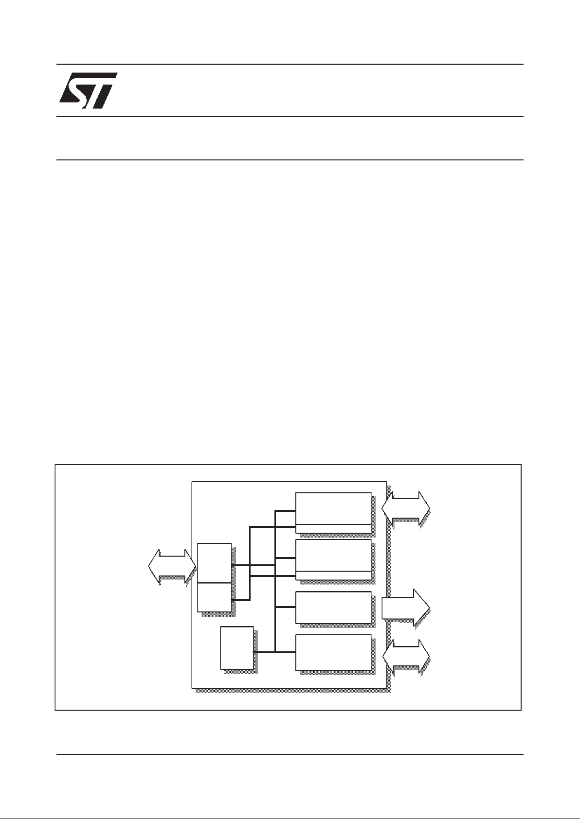
BLOCK DIAGRAM
Palette DAC
YUV - RGB,
Graphics Engine
128 bit 2D
Direct3D
8MByte
VGA
DMA Bus
Internal Bus
CCIR656
Video
PCI/AGP
128 bit
interface
Monitor/
TV
1.6 GByte/s
Internal Bus
Bandwidth
DMA Engine
Video Port
X & Y scaler
Host
Interface
FIFO/
DMA
Pusher
DMA Engine
SDRAM/SGRAM
Interface
KEY FEATURES
• Fast32-bit VGA/SVGA
• High performance 128-bit 2D/GUI/DirectDraw
Acceleration
• Interactive, Photorealistic Direct3D Accelera-
tion with advanced effects
• Pinout backwardscompatible with RIVA 128
• Massive 1.6Gbytes/s, 100MHz 128-bit wide
8MByte SGRAM framebufferinterface
• Adds 16Mbit SDRAM support for cost sensitive
8MByte framebuffer applications
• Video Acceleration for DirectDraw/DirectVideo,
MPEG-1/2 and Indeo
- Planar 4:2:0 and packed 4:2:2 Color Space
Conversion
- X and Y smooth up and down scaling
• 250MHz Palette-DAC supporting up to
1600x1200@85Hz
• NTSC and PAL output with flicker-filter
• Multi-function Video Port and serial interface
• Bus mastering DMA Accelerated Graphics Port
(AGP) 1.0 Interface supporting 133MHz 2X
data transfer mode
• Bus mastering DMA PCI 2.1 interface
• ACPI power management interface support
• 0.35 micron 5LM CMOS
• 300 PBGA
DESCRIPTION
The RIVA128ZX offers unparalleled 2D and 3D
performance, meeting all the requirements of the
mainstream PC graphics market and Microsoft’s
PC’97. RIVA128ZX combines all the features of
RIVA 128 plus 8MByte SDRAM and SGRAM
based framestore support and AGP2X datatransfer. It provides the most advanced Direct3D acceleration solution and delivers leadership VGA,
2D and Video performance, enabling a range of
applications from 3D games through to DVD, Intercast and video conferencing.

RIVA128ZX 128-BIT 3D MULTIMEDIA ACCELERATOR
TABLE OF CONTENTS
2/85
1 RIVA128ZX 300PBGA DEVICE PINOUT....................................................................................... 4
2 PIN DESCRIPTIONS ...................................................................................................................... 5
2.1 ACCELERATED GRAPHICS PORT (AGP) INTERFACE..................................................... 5
2.2 PCI 2.1 LOCALBUS INTERFACE........................................................................................ 5
2.3 FRAMEBUFFER INTERFACE .............................................................................................. 7
2.4 VIDEO PORT......................................................................................................................... 7
2.5 DEVICE ENABLE SIGNALS.................................................................................................. 8
2.6 DISPLAY INTERFACE.......................................................................................................... 8
2.7 VIDEO DAC AND PLL ANALOG SIGNALS .......................................................................... 8
2.8 POWER SUPPLY..................................................................................................................8
2.9 TEST...................................................................................................................................... 9
3 OVERVIEW OF THE RIVA128ZX .................................................................................................. 10
3.1 BALANCED PC SYSTEM...................................................................................................... 10
3.2 HOST INTERFACE ............................................................................................................... 10
3.3 2D ACCELERATION............................................................................................................. 11
3.4 3D ENGINE ........................................................................................................................... 11
3.5 VIDEO PROCESSOR............................................................................................................ 11
3.6 VIDEO PORT......................................................................................................................... 12
3.7 DIRECT RGB OUTPUT TO LOW COSTPAL/NTSC ENCODER ......................................... 12
3.8 SUPPORT FOR STANDARDS.............................................................................................. 12
3.9 RESOLUTIONS SUPPORTED.............................................................................................. 12
3.10 CUSTOMER EVALUATION KIT............................................................................................ 13
3.11 TURNKEY MANUFACTURING PACKAGE........................................................................... 13
4 ACCELERATED GRAPHICS PORT (AGP) INTERFACE ............................................................. 14
4.1 RIVA128ZX AGP INTERFACE.............................................................................................. 15
4.2 AGP BUS TRANSACTIONS.................................................................................................. 15
5 PCI 2.1 LOCAL BUS INTERFACE................................................................................................. 23
5.1 RIVA128ZX PCI INTERFACE ............................................................................................... 23
5.2 PCI TIMING SPECIFICATION............................................................................................... 24
6 FRAMEBUFFER INTERFACE ....................................................................................................... 30
6.1 SDRAM INTERFACE ............................................................................................................ 31
6.2 SGRAM INTERFACE............................................................................................................ 32
6.3 SDRAM/SGRAM ACCESSES AND COMMANDS................................................................ 35
6.4 LAYOUT OF FRAMEBUFFER CLOCK SIGNALS ................................................................ 37
6.5 FRAMEBUFFER INTERFACE TIMING SPECIFICATION.................................................... 37
7 VIDEO PLAYBACK ARCHITECTURE........................................................................................... 42
7.1 VIDEO SCALER PIPELINE................................................................................................... 43
8 VIDEO PORT.................................................................................................................................. 45
8.1 VIDEO INTERFACE PORT FEATURES............................................................................... 45
8.2 BI-DIRECTIONAL MEDIA PORT POLLING COMMANDSUSING MPC .............................. 46
8.3 TIMING DIAGRAMS.............................................................................................................. 47
8.4 656 MASTER MODE............................................................................................................. 51
8.5 VBI HANDLING IN THE VIDEO PORT ................................................................................. 52
8.6 SCALING IN THE VIDEO PORT........................................................................................... 52
9 BOOT ROM INTERFACE...............................................................................................................53

128-BIT 3D MULTIMEDIA ACCELERATOR RIVA128ZX
3/85
10 POWER-ON RESET CONFIGURATION........................................................................................ 55
11 DISPLAY INTERFACE................................................................................................................... 57
11.1 PALETTE-DAC ...................................................................................................................... 57
11.2 PIXEL MODES SUPPORTED ............................................................................................... 57
11.3 HARDWARE CURSOR......................................................................................................... 58
11.4 SERIAL INTERFACE.............................................................................................................59
11.5 ANALOG INTERFACE .......................................................................................................... 60
11.6 TV OUTPUT SUPPORT........................................................................................................ 61
12 IN-CIRCUIT BOARD TESTING...................................................................................................... 63
12.1 TEST MODES ....................................................................................................................... 63
12.2 CHECKSUM TEST................................................................................................................63
13 ELECTRICAL SPECIFICATIONS .................................................................................................. 64
13.1 ABSOLUTE MAXIMUM RATINGS ........................................................................................ 64
13.2 OPERATING CONDITIONS.................................................................................................. 64
13.3 DC SPECIFICATIONS........................................................................................................... 64
13.4 ELECTRICAL SPECIFICATIONS.......................................................................................... 65
13.5 DAC CHARACTERISTICS .................................................................................................... 65
13.6 FREQUENCY SYNTHESIS CHARACTERISTICS................................................................ 66
14 PACKAGE DIMENSION SPECIFICATION.................................................................................... 67
14.1 300 PIN BALL GRID ARRAY PACKAGE .............................................................................. 67
15 REFERENCES................................................................................................................................ 68
16 ORDERING INFORMATION .......................................................................................................... 68
APPENDIX............................................................................................................................................... 69
A PCI CONFIGURATION REGISTERS............................................................................................. 69
A.1 REGISTER DESCRIPTIONS FOR PCI CONFIGURATION SPACE .................................... 69

128-BIT 3D MULTIMEDIA ACCELERATORRIVA128ZX
4/85
1 RIVA128ZX 300PBGA DEVICE PINOUT
NOTES
1 NIC = No Internal Connection. Do not connect to these pins.
2 VDD=3.3V
∗ Signals denotedwith an asterisk are defined for future expansion. See
Pin Descriptions
, Section 2, page5 for details.
1234567891011121314151617181920
A
FBD[4] FBD[6] FBD[7] FBD[17] FBD[19] FBD[21] FBD[23] FBDQM[2] FBA[0] FBA[2] FBA[4] FBA[6] FBA[8] FBDQM[5] FBD[41] FBD[43] FBD[45] FBD[47] FBD[56] FBD[57]BFBD[3] FBD[5] FBD[16] FBD[18] FBD[20] FBD[22] FBDQM[0] FBA[9] FBA[1] FBA[3] FBA[5] FBA[7] FBCLK1 FBDQM[7] FBD[40] FBD[42] FBD[44] FBD[46] FBD[58] FBD[59]CFBD[1] FBD[2] FBD[28] FBD[27] FBD[26] FBD[25] FBD[15] FBD[13] FBD[11] FBD[9] FBDQM[1] FBWE# FBRAS# FBA[10] FBDQM[4] FBD[55] FBD[54] FBD[53] FBD[60] FBD[61]
D
FBCLK0 FBD[0] FBD[29] FBD[30] VDD FBD[24] FBD[14] FBD[12] FBD[10] FBD[8] FBDQM[3] FBCAS# FBCS0 FBCS1 FBDQM[6] VDD FBD[52] FBD[51] FBD[62] FBD[63]
E
SCL FBCLK2 FBD[31] VDD NIC VDD VDD VDD
FBCKE
∗ VDD VDD VDD VDD FBD[50] FBD[39] FBD[38]
F
MP_AD[6] NIC SDA FBCLKFB VDD VDD FBD[48] FBD[49] FBD[37] FBD[36]
G
MPFRAME# MP_AD[7] MP_AD[5] MP_AD[4] MPCLAMP VDD FBD[35] FBD[34] FBD[33] FBD[32]
H
MP_AD[2] MPSTOP# MPCLK MP_AD[3] VDD NIC FBDQM[12] FBDQM[14] FBDQM[15] FBDQM[13]
J
FBDQM[8] MPDTACK# MP_AD[1] MP_AD[0] GND GND GND GND FBD[118] FBD[119] FBD[105] FBD[104]KFBDQM[9] FBD[87] FBDQM[10] FBDQM[11] GND GND GND GND FBD[116] FBD[117] FBD[107] FBD[106]
L
FBD[86] FBD[85] FBD[72] FBD[73] GND GND GND GND FBD[114] FBD[115] FBD[109] FBD[108]MFBD[84] FBD[83] FBD[74] FBD[75] GND GND GND GND FBD[112] FBD[113] FBD[111] FBD[110]NFBD[82] FBD[81] FBD[76] FBD[77] NIC NIC FBD[102] FBD[103] FBD[121] FBD[120]PFBD[80] FBD[71] FBD[78] FBD[79] VDD VDD FBD[100] FBD[101] FBD[123] FBD[122]RFBD[70] FBD[69] FBD[88] FBD[89] NIC NIC FBD[98] FBD[99] FBD[125] FBD[124]TFBD[68] FBD[67] FBD[90] VDD NIC HOSTVDD HOSTVDD
HOST-
CLAMP
HOSTVDD
HOST-
CLAMP
HOSTVDD
HOST-
CLAMP
VDD FBD[97] FBD[127] FBD[126]
U
FBD[66] FBD[65] FBD[92] FBD[91]
HOST-
CLAMP
XTALOUT PCIRST# AGPST[1] PCIAD[30] PCIAD[26] PCICBE#[3] PCIAD[20] PCIAD[16] PCITRDY# PCIPAR HOSTVDD PCICBE#[0] FBD[96] VIDVSYNC VIDHSYNC
V
FBD[64] FBD[95] RED DACVDD VREF PCIINTA# PCIGNT# AGPPIPE# PCIAD[28] PCIAD[24] PCIAD[22] PCIAD[18] PCIFRAME# PCISTOP# PCIAD[15] PCIAD[11] PCIAD[6] PCIAD[2] TESTMODE ROMCS#WFBD[93] FBD[94] BLUE COMP PLLVDD PCIREQ# AGPST[2] PCIAD[31] PCIAD[27]
AGPAD-
STB1
PCIAD[21] PCIAD[17] PCIIRDY# PCICBE#[1] PCIAD[13] PCIAD[9] PCIAD[4] PCIAD[0] PCIAD[7] PCIAD[5]
Y
GREEN GND RSET XTALIN PCICLK AGPST[0]
PCIIDSEL/
AGPRBF#
PCIAD[29] PCIAD[25] PCIAD[23] PCIAD[19] PCICBE#[2]
PCI-
DEVSEL#
PCIAD[14] PCIAD[12] PCIAD[10] PCIAD[8]
AGPAD-
STB0
PCIAD[3] PCIAD[1]
128-BIT 3D MULTIMEDIA ACCELERATOR RIVA128ZX
5/85
2 PIN DESCRIPTIONS
2.1 ACCELERATED GRAPHICS PORT (AGP) INTERFACE
2.2 PCI 2.1 LOCAL BUS INTERFACE
Signal I/O Description
AGPST[2:0] I AGP status bus providing information fromthe arbiter to the RIVA128ZXon what it may
do. AGPST[2:0] only havemeaning to the RIVA128ZXwhen PCIGNT# is asserted. When
PCIGNT# is de-asserted these signals have no meaning and must beignored.
000 Indicates that previouslyrequested low priority read or flushdata is being
returned to the RIVA128ZX.
001 Indicates that previouslyrequested high priority readdata is being returned to
the RIVA128ZX.
010 Indicates that the RIVA128ZX is to provide low priority write data fora previous
enqueued write command.
011 Indicates that the RIVA128ZXis to provide high priority write data for a previous
enqueued write command.
100 Reserved
101 Reserved
110 Reserved
111 Indicates that the RIVA128ZX has been given permission to start a bus transac-
tion. The RIVA128ZXmay enqueue AGP requests by asserting AGPPIPE#or
start a PCI transaction by asserting PCIFRAME#. AGPST[2:0] are always an
output from the Core Logic (AGPchipset) and an input to the RIVA128ZX.
AGPRBF# O Read Buffer Full indicates when the RIVA128ZXis ready to accept previously requested
low priority read dataor not. When AGPRBF# is asserted the arbiter is not allowed to
return (low priority) read data to the RIVA128ZX.This signal should be pulled upvia a
4.7KΩ resistor (although it is supposed to be pulled up by the motherboard chipset).
AGPPIPE# O Pipelined Read is asserted byRIVA128ZX (when the current master) to indicate afull
width read addressis to be enqueued by the target.The RIVA128ZXenqueues one
request each rising clockedge while AGPPIPE#is asserted. When AGPPIPE#is deasserted no new requests are enqueued across PCIAD[31:0]. AGPPIPE# is a sustained
tri-state signal from the RIVA128ZXand is an inputto the target (the core logic).
AGPADSTB0,
AGPADSTB1
I/O Bus strobe signals providing timing for AGP2X data transfermode on PCIAD[15:00] and
PCIAD[31:16] respectively. The agent that is supplying data drives these signals.
Signal I/O Description
PCICLK I PCI clock. This signal provides timing forall transactions on the PCI bus, except for
PCIRST# and PCIINTA#. All PCI signals are sampled on the rising edgeof PCICLK and
all timing parametersare defined with respect to this edge.
PCIRST# I PCI reset. This signal is used to bring registers, sequencers and signalsto a consistent
state. When PCIRST# is asserted all output signals are tristated.
PCIAD[31:0] I/O 32-bit multiplexedaddress and data bus. A bus transactionconsists of anaddress phase
followedby one or more data phases.

128-BIT 3D MULTIMEDIA ACCELERATORRIVA128ZX
6/85
PCICBE[3:0]# I/O Multiplexedbus command and byte enable signals. During the address phase of a trans-
action PCICBE[3:0]# define the bus command, during the data phase PCICBE[3:0]# are
used as byte enables. The byte enables are validfor theentire data phase and determine
which bytelanes contain validdata. PCICBE[0]# applies tobyte 0 (LSB) and PCICBE[3]#
applies to byte 3 (MSB).
When connectedto AGPthese signals carry differentcommands thanPCI whenrequests
are beingenqueued using AGPPIPE#. Validbyte information isprovided during AGPwrite
transactions. PCICBE[3:0]# are not used during the return of AGP read data.
PCIPAR I/O Parity.This signal is the evenparity bit generated across PCIAD[31:0] and
PCICBE[3:0]#. PCIPAR is stable and valid one clock after the address phase. For data
phases PCIPAR is stable and validone clock after either PCIIRDY# is asserted on a write
transaction or PCITRDY# is asserted on a read transaction. OncePCIPARis valid, it
remains validuntil one clock after completion ofthe currentdataphase. The masterdrives
PCIPARfor address and write data phases; the target drives PCIPAR for read data
phases.
PCIFRAME# I/O Cycle frame.This signal is driven by the current master to indicate the beginning of an
access and itsduration. PCIFRAME# is asserted to indicate that a bustransaction is
beginning. Data transferscontinue whilePCIFRAME# is asserted. When PCIFRAME# is
deasserted, the transaction is in the finaldata phase.
PCIIRDY# I/O Initiator ready.This signalindicates theinitiator’s(bus master’s)ability to completethe cur-
rent data phase of the transaction. See extended description for PCITRDY#.
When connected toAGP this signal indicates theinitiator (AGPcompliant master) isready
to provideall write datafor the current transaction. Once PCIIRDY# is asserted for a write
operation, the master is not allowed to insert wait states. The assertion ofPCIIRDY# for
reads, indicates that the master is ready to transfera subsequent block of read data. The
master is never allowedto insert a wait state during the initial blockof a read transaction.
However, it may insert wait states after each blocktransfers.
PCITRDY# I/O Targetready. This signal indicates thetarget’s (selected device’s) ability to complete the
current data phaseof the transaction.
PCITRDY# is used in conjunction withPCIIRDY#. A data phase is completedon any clock
when both PCITRDY# and PCIIRDY# are sampled as being asserted. During a read,
PCITRDY# indicates that valid data ispresent on PCIAD[31:0]. During a write,it indicates
the target is prepared to accept data. Wait cycles are inserted until both PCIIRDY# and
PCITRDY# are asserted together.
When connectedtoAGP thissignal indicates theAGP complianttarget is ready to provide
read data for the entire transaction (when transaction cancomplete within four clocks) or
is ready to transfera (initialor subsequent) block of data, when the transfer requiresmore
than four clocks to complete. The target is allowed to insert wait states after each block
transfers on both read and write transactions.
PCISTOP# I/O PCISTOP# indicates that the current target is requesting the master to terminate the cur-
rent transaction.
PCIIDSEL I Initialization device select. This signal is used as a chip select during configuration read
and write transactions.
For AGP applicationsnote that IDSEL isnot a pin on the AGP connector. The RIVA128ZX
performs the deviceselect decode internally within its host interface. It is not required to
connect the AD16signal to the IDSEL pin as suggested in the AGP specification.
PCIDEVSEL# I/O Deviceselect. Whenacting as an output PCIDEVSEL#indicates that the RIVA128ZX has
decoded the PCI address and isclaiming the current access as the target. As an input
PCIDEVSEL# indicates whetherany other device on the bushas been selected.
PCIREQ# O Request. This signalis asserted by the RIVA128ZXto indicateto the arbiter that it desires
to become master of the bus.
Signal I/O Description
128-BIT 3D MULTIMEDIA ACCELERATOR RIVA128ZX
7/85
2.3 FRAMEBUFFER INTERFACE
2.4 VIDEO PORT
PCIGNT# I Grant. This signal indicates to the RIVA128ZX that access to the bus has been granted
and it can now become bus master.
When connectedto AGPadditional information isprovided on AGPST[2:0] indicating that
the master is the recipient of previously requested read data (high or low priority), it is to
provide write data (high or low priority), for a previously enqueued write command or has
been given permission to start a bus transaction (AGP or PCI).
PCIINTA# O Interrupt request line. This opendrain output is asserted and deasserted asynchronously
to PCICLK.
Signal I/O Description
FBD[127:0] I/O The 128-bitmemory data bus.
FBD[31:0] are also used to access up to 64KBytes of 8-bit ROM or Flash ROM, using
FBD[15:0] as address ROMA[15:0], FBD[31:24] as ROMD[7:0], FBD[17] as ROMWE#
and FBD[16] as ROMOE#.
FBA[10:0] O Memory Address bus. Configuration strapping options are also decoded on thesesignals
during PCIRST# as described in Section 10, page 55.
FBRAS# O Memory RowAddress Strobe forall memory devices.
FBCAS# O Memory ColumnAddress Strobe for all memory devices.
FBCS[1:0]# O Memory Chip Select strobes. For SDRAM the FBCS[1] pin providesthe memory’s inter-
nal bank select bit (BA/A11).
FBWE# O Memory Write Enablestrobe forall memory devices.
FBDQM[15:0] O Memory Data/Output Enable strobes.
FBCLK0,
FBCLK1,
FBCLK2
O Memory Clock signals. Separate clocksignals FBCLK0 and FBCLK1 are providedfor
each bank of memory forreduced clock skew and loading. Details ofrecommended memory clock layout are given in Section 6.4, page 37.
FBCLKFB I Framebuffer clock feedback. FBCLK2 is fed back to FBCLKFB.
FBCKE O Framebuffermemory clock enablesignal.
Signal I/O Description
MP_AD[7:0] I/O Media Port 8-bit multiplexedaddress and data bus or ITU-R-656 video data bus when in
656 mode.
MPCLK I 40MHz Media Port system clock or pixelclock when in 656 mode.
MPDTACK# I Media Port data transferacknowledgmentsignal.
MPFRAME# O Initiates Media Port transfers when active, terminates transferswhen inactive.
MPSTOP# I Media Port control signal used by the slave to terminate transfers.
Signal I/O Description
128-BIT 3D MULTIMEDIA ACCELERATORRIVA128ZX
8/85
2.5 DEVICE ENABLE SIGNALS
2.6 DISPLAY INTERFACE
2.7 VIDEO DAC AND PLL ANALOG SIGNALS
2.8 POWER SUPPLY
Signal I/O Description
ROMCS# O Enables reads from an external 64Kx 8 or 32Kx8 ROM or Flash ROM. This signalis used
in conjunction with framebuffer data lines as described abovein Section 2.3.
Signal I/O Description
SDA I/O Used forDDC2B+ monitor communication and interface to video decoder devices.
SCL I/O Used forDDC2B+ monitor communication and interface to video decoder devices.
VIDVSYNC O Vertical sync supplied to thedisplay monitor.No bufferingis required. In TV mode this sig-
nal supplies composite sync to an external PAL/NTSCencoder.
VIDHSYNC O Horizontal sync supplied to the display monitor. No buffering is required.
Signal I/O Description
RED,
GREEN,
BLUE
O RGB display monitor outputs. These are software configurableto drive either a doubly ter-
minated or singly terminated 75Ω load.
COMP - External compensation capacitor for the video DACs. This pin should be connected to
DACVDD via the compensation capacitor, see Figure 66, page 60.
RSET - A precision resistor placed between this pin and GND sets the full-scale video DAC cur-
rent, see Figure66, page 60.
VREF - A capacitor should beplaced between this pin and GND as shown in Figure 66, page 60.
XTALIN I A series resonantcrystal is connected between these two points to provide the reference
clock forthe internal MCLK andVCLK clock synthesizers,see Figure 66 and Table20,
page 60. Alternately, an externalLVTTLclock oscillator output may be driven into XTA-
LOUT, connecting XTALIN to GND.For designs supporting TV-out,XTALOUT should be
driven by a reference clock as described in Section 11.6, page 61.
XTALOUT O
Signal I/O Description
DACVDD P Analog power supply for the video DACs.
PLLVDD P Analog power supply forall clock synthesizers.
VDD P Digital power supply.
GND P Ground.
MPCLAMP P MPCLAMP is connected to +5V to protect the 3.3V RIVA128ZXfrom external devices
which will potentially drive 5V signal levels onto the Video Port input pins.
HOSTVDD P HOSTVDD is connected to the Vddq 3.3 pins on the AGP connector. This is the supply
voltage forthe I/O buffers and is isolated from the core VDD.On AGP designs these pins
are also connected to the HOSTCLAMP pins. On PCI designsthey are connected to the
3.3V supply.
HOSTCLAMP P HOSTCLAMP is the supply signalling rail protection for the host interface. In AGPdesigns
these signals areconnected to Vddq 3.3. For PCI designs they are connected to the I/O
power pins (V
(I/O)
).

128-BIT 3D MULTIMEDIA ACCELERATOR RIVA128ZX
9/85
2.9 TEST
Signal I/O Description
TESTMODE I For designs which will be tested in-circuit, this pin should be connected toGND through a
10KΩ pull-down resistor, otherwise this pin should be connected directly to GND.When
TESTMODE is asserted, MP_AD[3:0] are reassigned as TESTCTL[3:0] respectively.
Information on in-circuit test is given in Section 12, page 63.

128-BIT 3D MULTIMEDIA ACCELERATORRIVA128ZX
10/85
3 OVERVIEW OF THE RIVA128ZX
The RIVA128ZX is the first 128-bit 3D Multimedia
Accelerator to offer unparalleled 2D and 3D performance, meeting all the requirements of the
mainstream PC graphics market and Microsoft’s
PC’97. The RIVA128ZX introduces the most advanced Direct3D acceleration solution and also
delivers leadership VGA, 2D and Video performance, enabling a range of applications from 3D
games throughto DVD, Intercast and video conferencing.
3.1 BALANCED PC SYSTEM
The RIVA128ZX is designed to leverage existing
PC system resources such as system memory,
high bandwidth internal buses and bus master capabilities. The synergy between the RIVA128ZX
graphics pipeline architecture and that of the current generationPCI andnext generation AGPplatforms, defines ground breaking performance levels at the cost point currently required for mainstream PC graphics solutions.
Execute versus DMA models
The RIVA128ZXis architectedto optimize PC system resources in a manner consistent with the
AGP “Execute” model. In this model texturemap
data for 3D applications is stored in system memory and individual texels are accessed as needed
by the graphics pipeline. This is a significant enhancement over the DMA model where entire texture maps are transferred into off-screen framebuffer memory.
The advantages of the Execute versus the DMA
model are:
• Improved system performance since only the
required texels and not the entire texture map,
cross the bus.
• Substantial cost savings since all the frame-
buffer is usable for the displayed screen and Z
buffer andno part of it is required to be dedicated to texture storage or texture caching.
• There is no software overhead in the Direct3D
driver to manage texture caching between application memory and the framebuffer.
To extend the advantages of the Execute model,
the RIVA128ZX’s proprietary texture cache and
virtual DMA bus master design overcomes the
bandwidth limitation of PCI, by sustaining a high
texel throughput with minimum bus utilization.The
host interface supports burst transactions up to
133MHz and provides over 400MBytes/s onAGP.
AGP accesses offer other performance enhancements sincethey are fromnon-cacheable memory
(no snoop) and can be low priority to prevent processor stalls, or high priority to prevent graphics
engine stalls.
Building a balanced system
RIVA128ZX is architected to provide the level of
3D graphics performance and quality available in
top arcade platforms. To provide comparable
scene complexity in the 1997 time-frame, processors will have to achieve new levels of floating
point performance. Profiles have shown that 1997
mainstream CPUs will be able to transform over 1
million lit, meshed triangles/s at50% utilization using Direct3D. This represents an order of magnitude performance increase over anything attainable in 1996 PC games.
To build a balanced system the graphics pipeline
must match the CPU’sperformance.It mustbe capable of rendering at least 1 million polygons/s in
order to avoid CPU stalls. Factors affecting this
system balance include:
• Direct3D compatibility. Minimizing the differ-
ences between the hardware interface and the
Direct3D data structures.
• Triangle setup. Minimizing the number of for-
mat conversionsand delta calculations done by
the CPU.
• Display-list processing. Avoiding CPU stalls by
allowing the graphics pipeline to execute independently of the CPU.
• Vertex caching. Avoids saturating the host in-
terface withrepeated vertices, lowering thetraffic onthe busandreducing systemmemory collisions.
• Host interface performance.
3.2 HOST INTERFACE
The host interfaceboosts communicationbetween
the host CPU and the RIVA128ZX. The optimized
interface performs burst DMA bus mastering for
efficient and fast data transfer.
• 32-bit PCI version 2.1 or AGP version 1.0
• Burst DMA Master and target
• 33MHz PCI clock rate, 66MHz AGP clock rate
and AGP 2X mode
• Supports over 100MBytes/s with33MHz PCI to
over 400MBytes/s on AGP 2X mode
• Implements read buffer posting on AGP

128-BIT 3D MULTIMEDIA ACCELERATOR RIVA128ZX
11/85
•
Fully supportsthe “Execute” modelon both PCI
and AGP
3.3 2D ACCELERATION
The RIVA128ZX’s 2D rendering engine delivers
industry-leading Windows acceleration performance:
• 100MHz 128-bit graphics engine optimized for
single cycle operation into the 128-bit memory
interface supporting up to 1.6GBytes/s
• Acceleration functions optimized for minimal
software overhead on key GDI calls
• Extensive support for DirectDraw in
Windows95 including optimized Direct Framebuffer (DFB) access with Write-combining
• Accelerated primitives including BLT, transpar-
ent BLT, stretchBLT, points, lins, lines,
polylines, polygons, fills, patterns, arbitrary
rectangular clipping and improved text rendering
• Pipeline optimized for multiple color depths in-
cluding 8, 15, 24, and 30 bits per pixel
• DMA Pusher allows the 2Dgraphics pipeline to
load rendering methods optimizing
RIVA128ZX/host multi-tasking
• Execution of all 256 Raster Operations (as de-
fined by Microsoft Windows) at 8, 15, 24 and
30-bit color depths
• 15-bit hardware color cursor
• Hardware color dithering
• Multi buffering (Double, Triple, Quad buffering)
for smooth animation
3.4 3D ENGINE
Triangle setup engine
• Setup hardware optimized for Microsoft’s
Direct3D API
• 5Gflop floating point geometry processor
• Slope and setup calculations
• Accepts IEEE Single Precision format used in
Direct3D
• Efficient vertex caching
Rendering engine
The RIVA128ZX Multimedia Accelerator integrates an orthodox 3D rendering pipeline and triangle setup function which not only fully utilizes
the capabilities of the Accelerated Graphics Port,
but also supports advanced texture mapped 3D
over the PCI bus. The RIVA128ZX 3D pipeline of-
fers to Direct3D or similar APIs advanced triangle
rendering capabilities:
• Rendering pipeline optimized for Microsoft’s
Direct3D API
• Perspective correct true-color Gouraud lighting
and texture mapping
• Full 32-bit RGBA texture filter and Gouraud
lighting pixel data path
• Alpha blending for translucency and transpar-
ency
• Sub-pixel accurate texture mapping
• Internal pixel path: up to 24bits, alpha: up to 8
bits
• Texture magnification filtering with high quality
bilinear filtering without performance degradation
• Texture minification filtering with MIP mapping
without performance degradation
• LOD MIP-mapping: filter shape is dynamically
adjusted based on surface orientation
• Texture sizes from 4 to 2048 texels in either U
or V
• Textures can be looped and paged in real time
for texture animation
• Perspective correct per-pixel fog for atmo-
spheric effects
• Perspective correct specular highlights
• Multi buffering (Double, Triple, Quad buffering)
for smooth 3D animation
• Multipass rendering for environmental mapping
and advanced texturing
3.5 VIDEO PROCESSOR
The RIVA128ZX Palette-DAC pipeline accelerates
full-motion video playback, sustaining 30 frames
per secondwhile retaining the highestquality color
resolution, implementing true bilinear filtering for
scaled video, and compensating for filtering losses
using edge enhancement algorithms.
• Advanced support for DirectDraw (DirectVideo)
in Windows 95
• Back-end hardwarevideo scalingfor video con-
ferencing and playback
• Hardware color space conversion (YUV 4:2:2
and 4:2:0)
• Multi-tap X and Y filtering for superior image
quality
• Optional edge enhancement to retain video
sharpness

128-BIT 3D MULTIMEDIA ACCELERATORRIVA128ZX
12/85
•
Supportfor scaledfield interframingfor reduced
motion artifacts and reduced storage
• Per-pixel color keying
• Multiple video windows with hardware color
space conversion and filtering
• Planar YUV12 (4:2:0) to/from packed (4:2:2)
conversion for software MPEG acceleration
and H.261 video conferencing applications
• Accelerated playback of industry standard co-
decs including MPEG-1/2, Indeo, Cinepak
3.6 VIDEO PORT
The RIVA128ZX Multimedia Accelerator provides
connectivity forvideo input devices suchas Philips
SAA7111A, ITT 3225 and Samsung KS0127
through an ITU-R-656 video input bus to DVD and
MPEG2 decodersthrough bidirectional mediaport
functionality.
• Supported through VPE extensions to Direct-
Draw
• Supports filtered down-scaling and decimation
• Supports real time video capture via Bus Mas-
tering DMA
• Serial interface for decoder control
3.7 DIRECT RGB OUTPUT TO LOW COST
PAL/NTSC ENCODER
The RIVA128ZX has also been designed to interface to a standard PAL or NTSC television via a
low cost TVencoder chip. InPAL or NTSC display
modes the interlaced output is internally flicker-filtered and CCIR/EIA compliant timing reference
signals are generated.
3.8 SUPPORT FOR STANDARDS
• Multimedia support for MS-DOS, Windows
3.11, Windows 95, and Windows NT
• Acceleration for Windows 95 Direct APIs in-
cluding Direct3D, DirectDraw and DirectVideo
• VGA and SVGA: The RIVA128ZX has an in-
dustry standard32-bit VGAcore andBIOS support. In PCI configuration space the VGA can
be enabled and disabled independently of the
GUI.
• Glue-less Accelerated Graphics Port (AGP 1.0)
or PCI 2.1 bus interface
• ITU/CCIR-656 compatible video port
• VESA DDC2B+, DPMS, VBE 2.0 supported
3.9 RESOLUTIONS SUPPORTED
Resolution BPP 2MByte 4MByte (128-bit) 8MByte (64-bit) 8MByte (128-bit)
640x480
4 120Hz 120Hz 120Hz 120Hz
8 120Hz 120Hz 120Hz 120Hz
16 120Hz 120Hz 120Hz 120Hz
32 120Hz 120Hz 120Hz 120Hz
800x600
8 120Hz 120Hz 120Hz 120Hz
16 120Hz 120Hz 120Hz 120Hz
32 120Hz 120Hz 120Hz 120Hz
1024x768
8 120Hz 120Hz 120Hz 120Hz
16 120Hz 120Hz 120Hz 120Hz
32 - 120Hz 120Hz 120Hz
1152x864
8 120Hz 120Hz 120Hz 120Hz
16 120Hz 120Hz 120Hz 120Hz
32 - 100Hz 100Hz 100Hz
1280x1024
8 100Hz 100Hz 100Hz 100Hz
16 - 100Hz 100Hz 100Hz
32 - - t.b.d. 75Hz
1600x1200
8 85Hz 85Hz 85Hz 85Hz
16 - 85Hz 85Hz 85Hz
32 - - - 60Hz
1920x1080
8 - 85Hz 85Hz 85Hz
16 - - 85Hz 85Hz
1920x1200
8 - 75Hz 75Hz 75Hz
16 - - 75Hz 75Hz
1800x1440 16 - - 60Hz 60Hz

128-BIT 3D MULTIMEDIA ACCELERATOR RIVA128ZX
13/85
3.10 CUSTOMER EVALUATION KIT
A Customer Evaluation Kit (CEK) is available for
evaluating the RIVA128ZX. The CEK includes a
PCI or AGP adapter card designed to support the
RIVA128ZX feature set, an evaluation CD-ROM
containing afast-installation application, extensive
device drivers and programs demonstrating the
RIVA128ZX features and performance.
This CEK includes:
• RIVA128ZX evaluation board and CD-ROM
• QuickStart install/user guide
• OS drivers and files
- Windows 3.11
- Windows 95 Direct X/3D
- Windows NT 3.5
- Windows NT 4.0
• Demonstration files and Game demos
• Benchmark programs and files
3.11 TURNKEY MANUFACTURING PACKAGE
A Turnkey Manufacturing Package (TMP) isavail-
able to support OEM designs and development
through to production. It delivers a complete manufacturable hardware and software solution that
allows an OEM to rapidly design and bring to volume an RIVA128ZX-based product.
This TMP includes:
• CD-ROM
- RIVA128ZX Datasheet and Application
Notes
- OrCAD schematic capture and PADS
layout design information
- Quick Start install/user guide/releasenotes
- BIOS Modification program, BIOS binaries,
utilities and BIOS Modification Guide documentation
- Bring-up and OEM Production Diagnostics
- Software and Utilities
• OS drivers and files
- Windows 3.11
- Windows 95 Direct X/3D
- Windows NT 3.5
- Windows NT 4.0
• Content developer and WWW information
• Partner solutions
• Access to our password-protected web site for
upgrade files and release notes.
128-BIT 3D MULTIMEDIA ACCELERATORRIVA128ZX
14/85
4 ACCELERATED GRAPHICS PORT (AGP) INTERFACE
The AcceleratedGraphics Port (AGP) is ahigh performance,component level interconnecttargeted at3D
graphical display applications and based on performance enhancements to the PCI local bus.
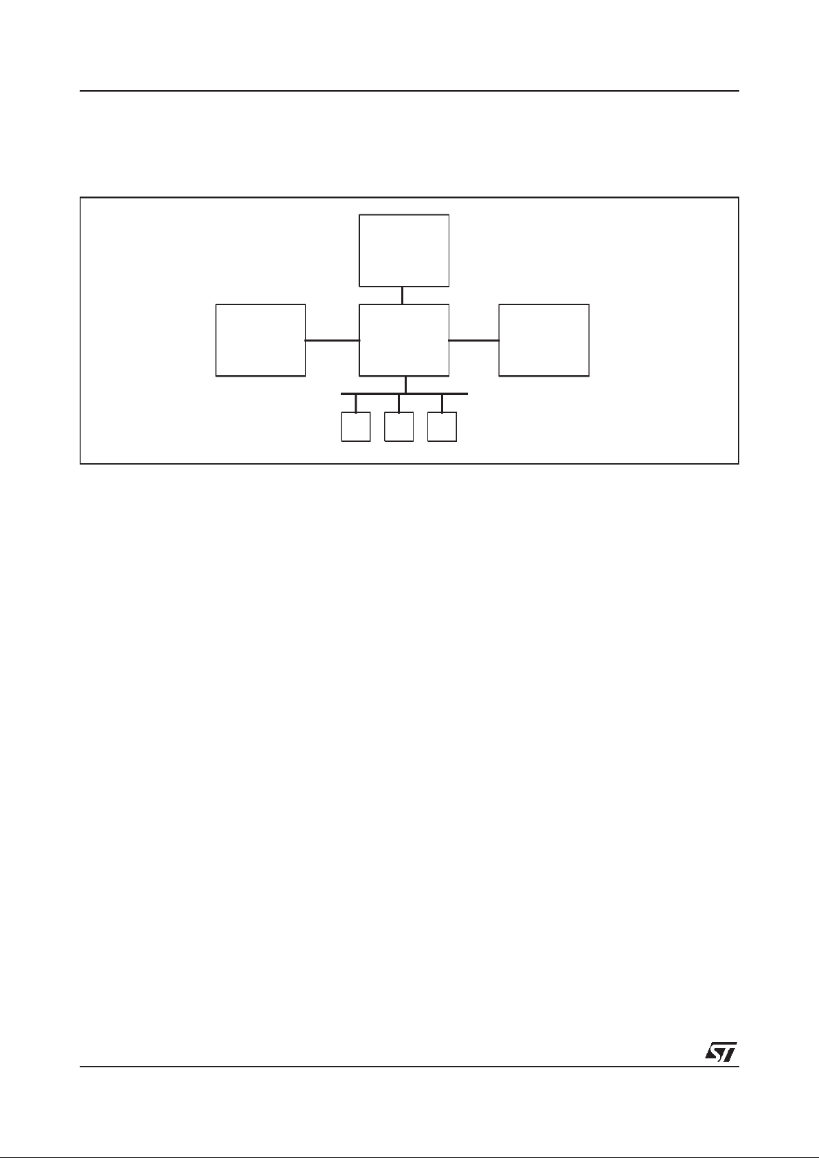
Figure 1. System block diagram showing relationship between AGP and PCI buses
Background to AGP
Although 3D graphics acceleration is becoming a
standard feature of multimedia PC platforms, 3D
rendering generally has a voracious appetite for
memory bandwidth.Consequently thereis upward
pressure onthe PC’s memory requirement leading
to higher billof materialcosts. These trends will increase, requiring high speed access to larger
amounts of memory. The primary motivation for
AGP therefore was to contain these costs whilst
enabling performance improvements.
By providing significant bandwidth improvement
between the graphics accelerator and system
memory, someof the3D renderingdata structures
can be shifted into main memory, thus relieving
the pressure to increase the cost of the local
graphics memory.
Texture data are the first structures targeted for
shifting to system memory for four reasons:
1 Textures are generally read only, and therefore
do not have special access ordering or coherency problems.
2 Shifting textures balances the bandwidth load
between system memory and local graphics
memory, since a well cached host processor
has much lower memory bandwidth requirements than a 3D rendering engine. Texture accesscomprises perhapsthe largestsingle component of rendering memory bandwidth (compared with rendering,display and Z buffers), so
avoiding loading or cachingtexturesin graphics
local memory saves not only this component of
local memory bandwidth, but also the bandwidth necessary to load the texture store in the
first place. Furthermore, this data must pass
through main memory anyway as it is loaded
from a mass store device.
3 Texture size is dependent upon application
quality rather than on display resolution, and
therefore subject to the greatest pressure for
growth.
4 Texture data is not persistent; it resides in
memory only for the duration of the application,
so any system memory spent on texture storage can be returned to the free memory heap
when the application finishes (unlike display
buffers which remain in use).
Other data structures can be moved tomain memory but the biggest gain results from moving texture data.
Relationship of AGP to PCI
AGP is a superset of the 66MHzPCI Specification
(Revision 2.1) with performance enhancements
optimized for highperformance 3D graphics applications.
The PCI Specification is unmodified by AGP and
‘reserved’ PCI fields, encodings and pins, etc. are
not used.
AGP does not replace the need for the PCI bus in
the system and the two are physically, logically,
and electrically independent.As shown in Figure1
AGP chipsetRIVA128ZX
System
memory
CPU
I/O I/O I/O
PCI
AGP
128-BIT 3D MULTIMEDIA ACCELERATOR RIVA128ZX
15/85
the AGP bridge chip and RIVA128ZX are the only
devices on theAGP bus - all other I/O devices remain on the PCI bus.
The add-in slot defined for AGP uses a new connector body (for electrical signaling reasons)
which is not compatible with the PCI connector;
PCI and AGP boards are not mechanically interchangeable.
AGP accesses differ from PCI in that they are
pipelined. This compares with serialized PCI
transactions, where the address, wait and data
phases need to complete before the next transaction starts. AGP transactionscan only accesssystem memory - not other PCI devices or CPU. Bus
mastering accesses can be either PCI or AGPstyle.
Full details of AGP are given in the
Accelerated
Graphics Port InterfaceSpecification
[3] published
by Intel Corporation.
4.1 RIVA128ZX AGP INTERFACE
The RIVA128ZX glueless interface to AGP1.0 is shown in Figure 2.
Figure 2. AGP interface pin connections
4.2 AGP BUS TRANSACTIONS
AGP bus commands supported
The following AGP bus commands are supported
by the RIVA128ZX:
- Read
- Read (hi-priority)
PCI transactions on the AGP bus
PCI transactions can be interleaved with AGP
transactions including between pipelined AGP
data transfers.A basic PCItransaction ontheAGP
interface is shown in Figure 3. If the PCI target is
a non AGP compliant master, it will not see
AGPST[2:0] and the transaction appears to be on
a PCI bus. For AGP aware bus masters,
AGPST[2:0] indicate thatpermission touse theinterface has been granted to initiate a request and
not to move AGP data.
AGP bus
PCICBE[3:0]#
PCIAD[31:0]
AGPPIPE#
32
4
PCIDEVSEL#
PCIIRDY#
PCITRDY#
PCISTOP#
PCIIDSEL
PCIREQ#
PCIGNT#
PCICLK
PCIRST#
PCIPAR
PCIINTA#
RIVA128ZX
AGPST[2:0]#
3
AGPRBF#
128-BIT 3D MULTIMEDIA ACCELERATORRIVA128ZX
16/85
Figure 3. Basic PCI transaction on AGP
An example of a PCI transaction occurring between an AGP command cycle and return of data is shown
in Figure 4. This shows the smallest number of cycles during which an AGPrequest can be enqueued, a
PCI transaction performed and AGP read data returned.
Figure 4. PCI transaction occurring between AGP request and data
bus cmd
data_pciaddress
BE[3:0]#
111 111 xxx xxx xxxxxx
PCICLK
PCIFRAME#
PCIAD[31:0]
PCICBE[3:0]#
PCIIRDY#
PCITRDY#
PCIDEVSEL#
PCIREQ#
PCIGNT#
AGPST[2:0]
134562
A9
111 xxx 111 111 xxx111
address data D7 +1
C9 pci_cmd BE 0000 000
xxx 00x xxx xxx
PCICLK
AGPPIPE#
PCIFRAME#
PCIAD[31:0]
PCICBE#
PCIIRDY#
PCITRDY#
PCIDEVSEL#
PCIAGPRBF#
PCIREQ#
PCIGNT#
AGPST[2:0]
1 2345678910
128-BIT 3D MULTIMEDIA ACCELERATOR RIVA128ZX
17/85
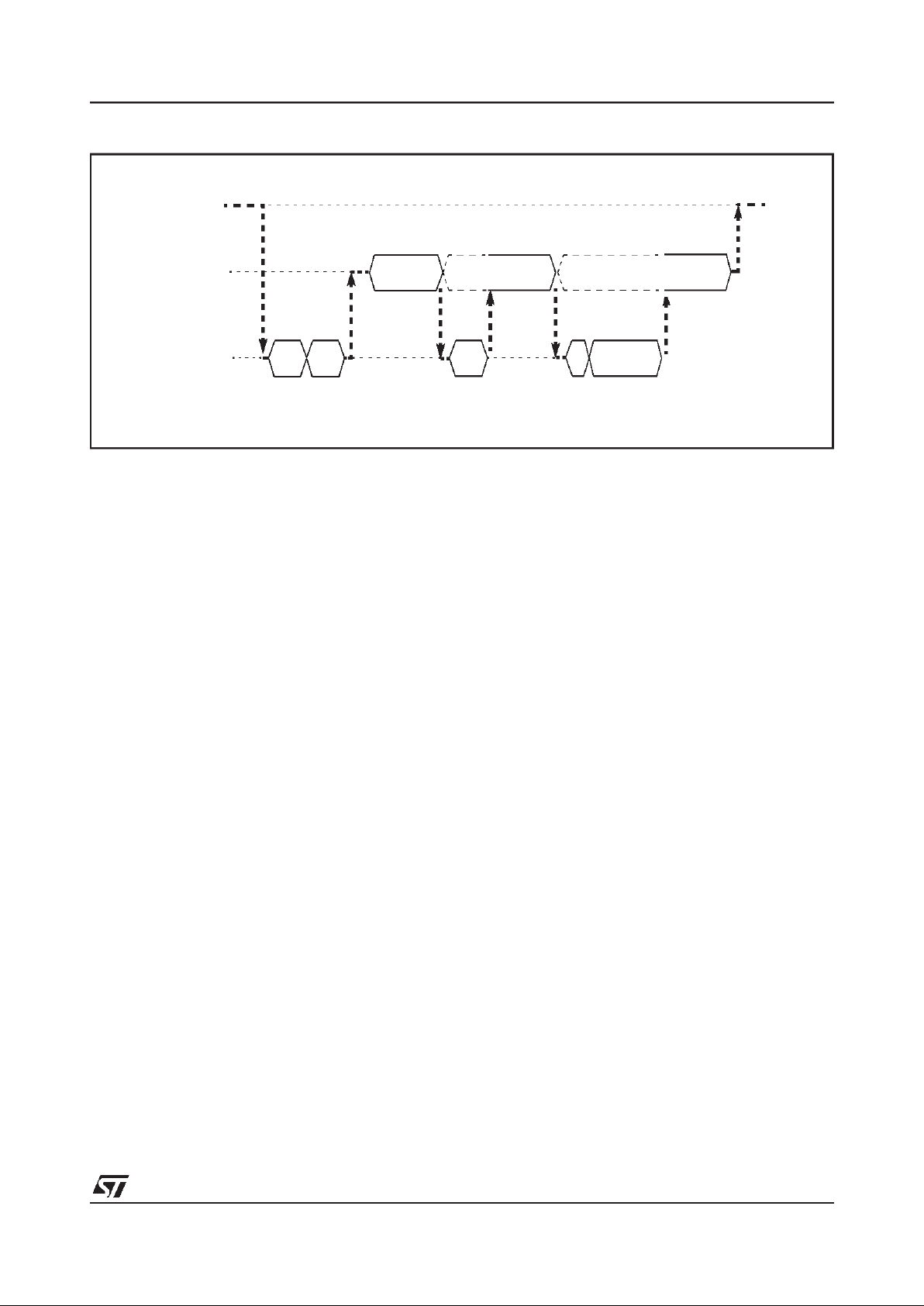
Figure 5. Basic AGP pipeline concept
Pipeline operation
Memory access pipelining provides the main performance enhancement of AGP over PCI. AGP
pipelined bus transactions share most of the PCI
signal set, and are interleaved with PCI transactions on thebus.
The RIVA128ZX supports AGP pipelined reads
with a 4-deep queue of outstanding read requests.
Pipelined reads are primarily used by the
RIVA128ZX for cache filling, the cache size being
optimized for AGP bursts. Depending on the AGP
bridge, abandwidth ofup to 248MByte/s isachievable for 128-byte pipelined reads. This compares
with around 100MByte/s for 128-byte 33MHz PCI
reads. Another feature of AGP is that for smaller
sized reads the bandwidth is not significantly reduced. Whereas 16-byte reads on PCI transfer at
around 33MByte/s, on AGP around 175MByte/s is
achievable. The RIVA128ZX actually requests
reads greater than 64 bytes in multiplesof 32-byte
transactions.
The pipedepth canbe maintained bythe AGP bus
master (RIVA128ZX) intervening in a pipelined
transfer to insert new requests between data replies. This bus sequencing is illustrated in Figure
5.
When the bus is in an idle condition, the pipe can
be started by inserting one or more AGP access
requests consecutively. Once the data reply to
those accesses starts, that stream can be broken
(or intervened) by the busmaster (RIVA128ZX) inserting one or more additional AGP access requests or inserting a PCI transaction. This intervention is accomplished with the bus ownership
signals, PCIREQ# and PCIGNT#.
The RIVA128ZX implements both high and low
priority reads depending of the status of the rendering engine. Ifthe pipeline is likely to stall due to
system memory read latency, a high priority read
request is posted.
Address Transactions
The RIVA128ZX requests permission from the
bridge to use PCIAD[31:0] to initiate either an
AGP request or a PCI transaction by asserting
PCIREQ#. The arbiter grants permission by asserting PCIGNT# with AGPST[2:0] equal to ”111”
(referred to as START). Whenthe RIVA128ZX receives START it must start thebus operation within two clocks of the bus becoming available. For
example, whenthe busis inan idle conditionwhen
START is received, the RIVA128ZX must initiate
the bus transaction on the next clock and the one
following.
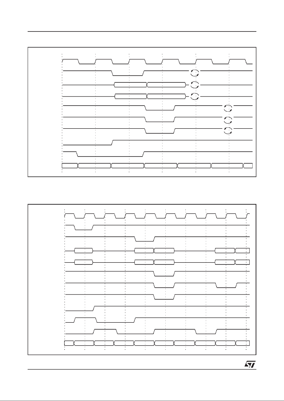
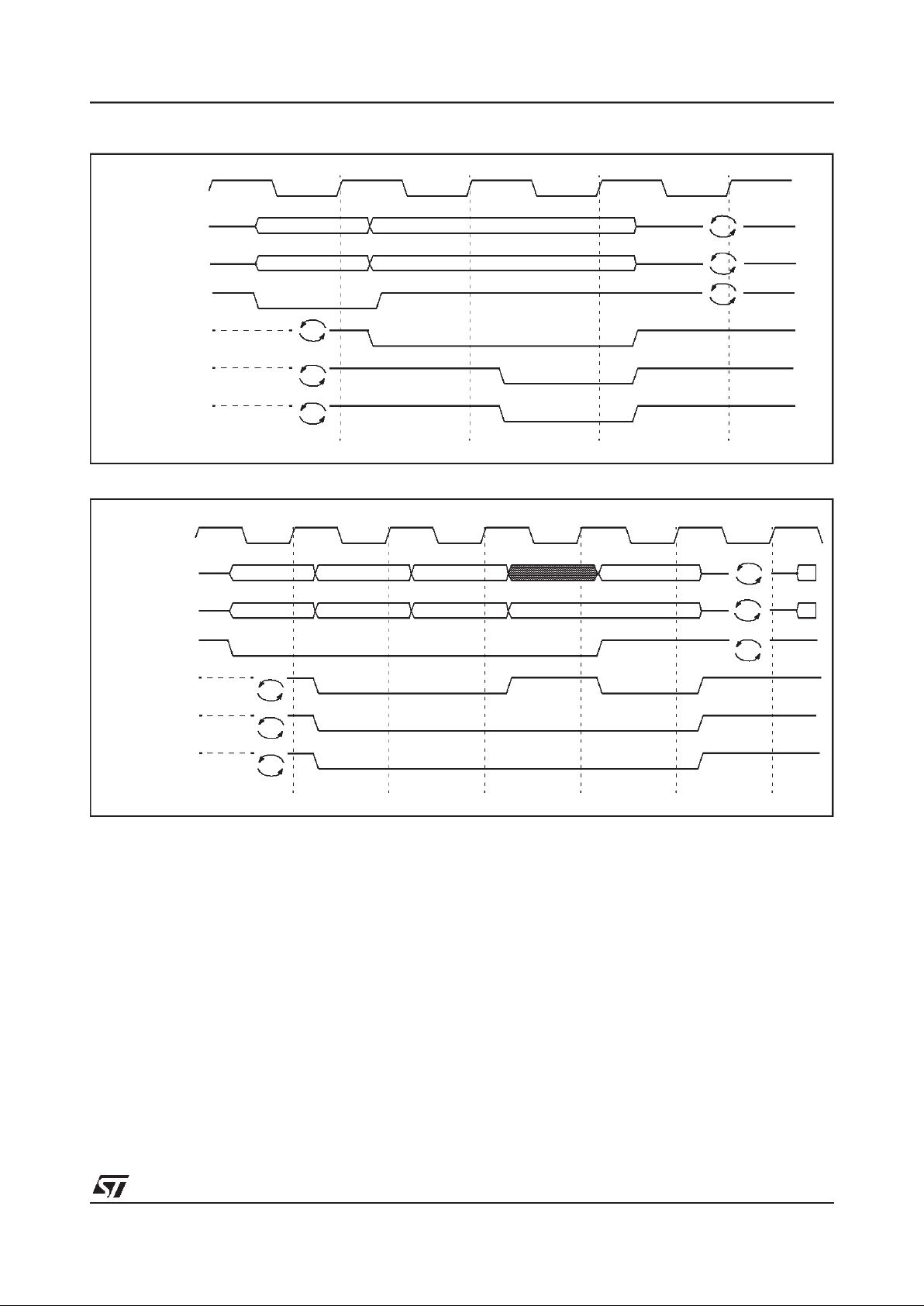
Figure 6 shows a single address being enqueued
by the RIVA128ZX. Sometime before clock 1, the
RIVA128ZX asserts PCIREQ# to gain permission
to usePCIAD[31:0]. Thearbiter grants permission
by indicating START on clock 2. A new request
(address, command and length) are enqueued on
each clock in which AGPPIPE# is asserted. The
address of the request tobe enqueued is presented onPCIAD[31:3], thelength on PCIAD[2:0] and
the command on PCICBE[3:0]#. In Figure 6 only
a single address is enqueued since AGPPIPE# is
just asserted for a single clock. The RIVA128ZX
indicates that the current address is the last it intends to enqueue when AGPPIPE# is asserted
and PCIREQ# is deasserted (occurring on clock
3). Once the arbiter detects the assertion of AGP-
PIPE# or PCIFRAME# it deasserts PCIGNT# on
clock 4.
Bus Idle
Pipelined
data
transfer
Intervene
cycles
Pipelined AGP requests
A1 A2
Data-1 Data-2
A3
PCI transaction
A
Data
Data-3
128-BIT 3D MULTIMEDIA ACCELERATORRIVA128ZX
18/85
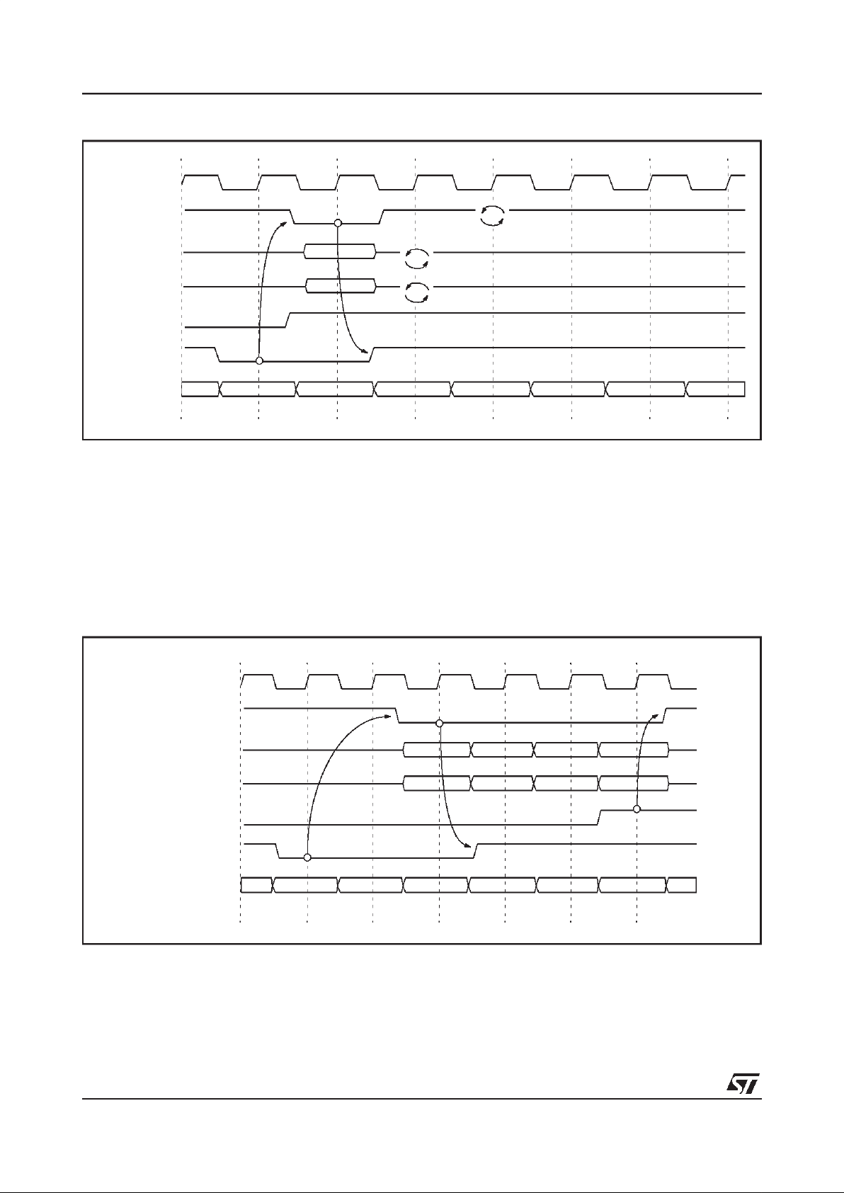
Figure 6. Single address - no delay by master
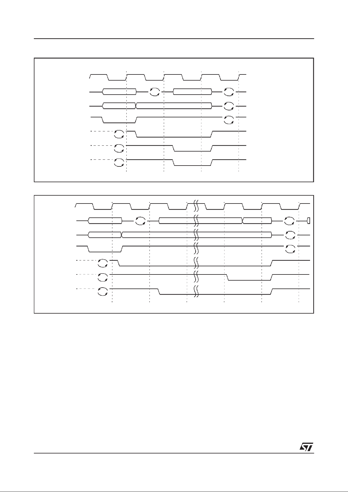
Figure 7 showsthe RIVA128ZXenqueuing 4 requests, where the first request is delayed bythe maximum
2 cycles allowed. START is indicated on clock 2, but the RIVA128ZX does not assert AGPPIPE# until
clock 4. Note that PCIREQ# remainsasserted on clock 6 toindicate that thecurrent request is not the last
one. When PCIREQ# is deasserted onclock 7 with AGPPIPE# still assertedthis indicates thatthe current
address is the last one tobe enqueuedduring thistransaction. AGPPIPE# must be deassertedon thenext
clock when PCIREQ# is sampled as deasserted. If the RIVA128ZXwants to enqueue more requestsduring this bus operation, itcontinues assertingAGPPIPE# until all ofits requests areenqueued or until it has
filled all the available request slots provided by the target.
Figure 7. Multiple addresses enqueued, maximum delay by RIVA128ZX
2X Data Transfers
2X data transfers are similar to 1X transfers except that an entire 8 bytes are transferred during a single
PCICLK period. This requires that two 4 byte pieces of data are transferred acrossPCIAD[31:0] for each
CLK period. A read data transfer is described followed by awrite transfer.
C1
A1
111 111 xxx xxx xxxxxx xxx xxx
PCICLK
AGPPIPE#
PCIAD[31:0]
PCICBE[3:0]#
PCIREQ#
PCIGNT#
AGPST[2:0]
12345678
A1
111 111 111 xxx xxxxxx xxx xxx
A2 A3 A4
C1 C2 C3 C4
PCICLK
AGPPIPE#
PCIAD[31:0]
PCICBE#
PCIREQ#
PCIGNT#
AGPST[2:0]
1234567
128-BIT 3D MULTIMEDIA ACCELERATOR RIVA128ZX
19/85
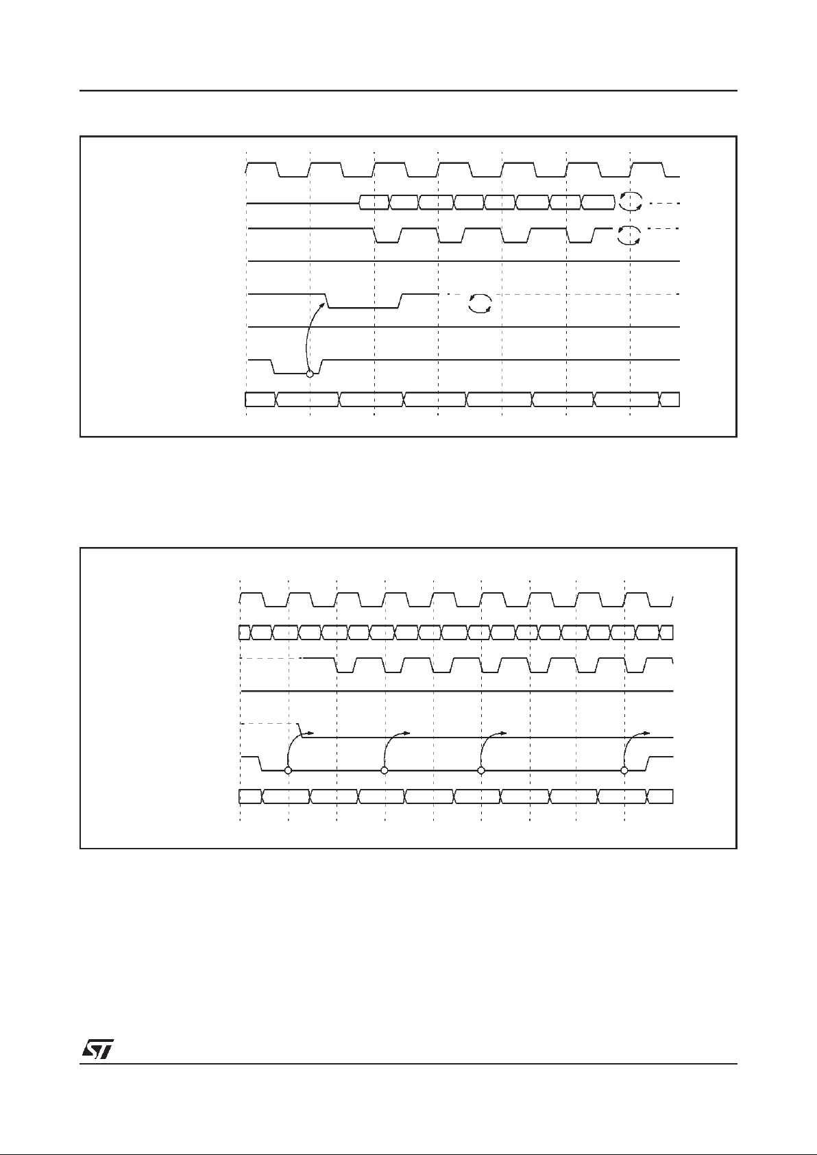
Figure 8. 2X Read data, no delay
Figure 8shows 32 bytes being transferred during 4 clocks(compared with 16bytes inAGP 1x mode). The
control signals are identical. The AGPAD_STBx signal has been added when data is transferred at 8
bytes per PCICLK period. AGPAD_STBx represents AGPAD_STB0 and AGPAD_STB1 and are used
by the2X interface logicto indicatewhen valid data ispresenton theAD bus.Thecontrol logic (PCITRDY#
in this case) indicates when data can be used by the target.
Figure 9. 2X Back to back read data, no delay
Figure 9 showsback to back 8 byteread transactions. AGPST[2:0]are shown toggling between “000”and
“001” to illustrate thatthey are actually changing. However, theyare not required to change between high
and low priority to do back to back transactions. In this diagram, PCITRDY# is asserted on each clock
since a new transaction starts on each clock.
+1
00x xxx xxx xxx xxxxxx xxx
R1 +5 +6 +7+2 +3 +4
PCICLK
PCIAD[31:0]
AGPADSTBx
AGPRBF#
PCITRDY#
PCIREQ#
PCIGNT#
AGPST[2:0]
1234567
+1
000 001 000 001 000xx 001 000 001
L6 +1 H5 +1
xx
H4 +1 +L7 L8 +1 H6 +1 L9 +1
PCICLK
PCIAD[31:0]
AGPADSTBx
AGPRBF#
PCITRDY#
PCIGNT#
AGPST[2:0]
123456789

128-BIT 3D MULTIMEDIA ACCELERATORRIVA128ZX
20/85
Figure 10. 2X Basic write no delay
Figure 10is a basic write transaction thattransfers data at the2X rate. There is no difference in the control
signals from AGP 1x mode - only more data is moved. The normal control signals determine when data is
valid.
Figure 11. QuadWord writes back to back - no delays
Figure 11 illustratesmultiple 8 bytewrite operationscompared with thesingle transfer shownin Figure 10.
When the transactions are short, thearbiter is required to give grants onevery clock or the AD bus willnot
be totally utilized.In this examplea new writeis started on eachrising clock edgeexcept clock 7,because
the arbiter deasserted PCIGNT# on clock 6. Since a new transaction is started on each CLK, PCIIRDY#
is only deasserted on clock 7.
xxx xxx 01x xxx xxxxx xxx xxx xxx
+2 +3 +4W1 +1 +5 +6 +7
BE BE BEBE BE BE BE BE
PCICLK
PCIAD[31:0]
PCICBE#
AGPADSTBx
PCIIRDY#
PCITRDY#
PCIREQ#
PCIGNT#
AGPST[2:0]
123456789
01x 01x 01x 01x xxxxx 01x 01x xxx
W6 +1
x
W5 +1 W7 +1W3 +1 W4 +1 W8 +1
BE BEBE BE BE BEBE BE BE BE BE BE
PCICLK
PCIAD[31:0
]
PCICBE#
AGPADSTBx
PCIIRDY#
PCITRDY#
PCIGNT#
AGPST[2:0]
123456789
128-BIT 3D MULTIMEDIA ACCELERATOR RIVA128ZX
21/85
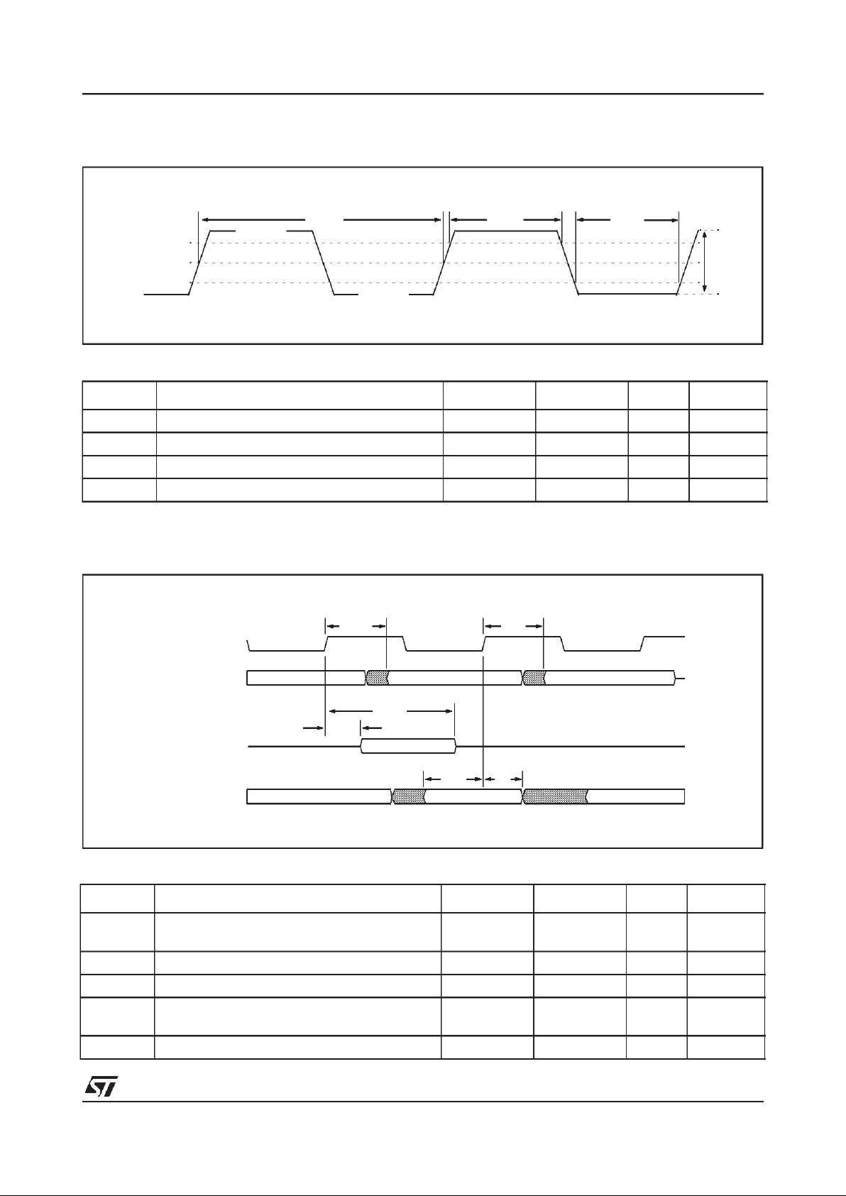
AGP timing specification
Figure 12. AGP clock specification
Table 1. AGP clock timing parameters
NOTES
1 This rise and fall time is measured across the minimum peak-to-peak range as shown in Figure12.
Figure 13. AGP timing diagram
Table 2. AGP timing parameters
Symbol Parameter Min. Max. Unit Notes
t
CYC PCICLK period 15 30 ns
t
HIGH PCICLK high time 6 ns
t
LOW PCICLK low time 6 ns
PCICLK slew rate 1.5 4 V/ns 1
Symbol Parameter Min. Max. Unit Notes
t
VAL AGPCLK to signal valid delay (data and control
signals)
211ns
t
ON Float to active delay 2 ns
t
OFF Active to float delay 28 ns
t
SU Input set up time to AGPCLK (data and control
signals)
7ns
t
HInput hold time from AGPCLK 0ns
t
CYC tHIGH tLOW
PCICLK
0.3VDD
0.4VDD
0.5VDD
0.2VDD
0.6VDD
2V p-to-p
(minimum)
tVAL
tVAL
tON
tOFF
tSU
tH
data1 data2
data1 data2
AGPCLK
Output delay
Tri-state output
Input
128-BIT 3D MULTIMEDIA ACCELERATORRIVA128ZX
22/85
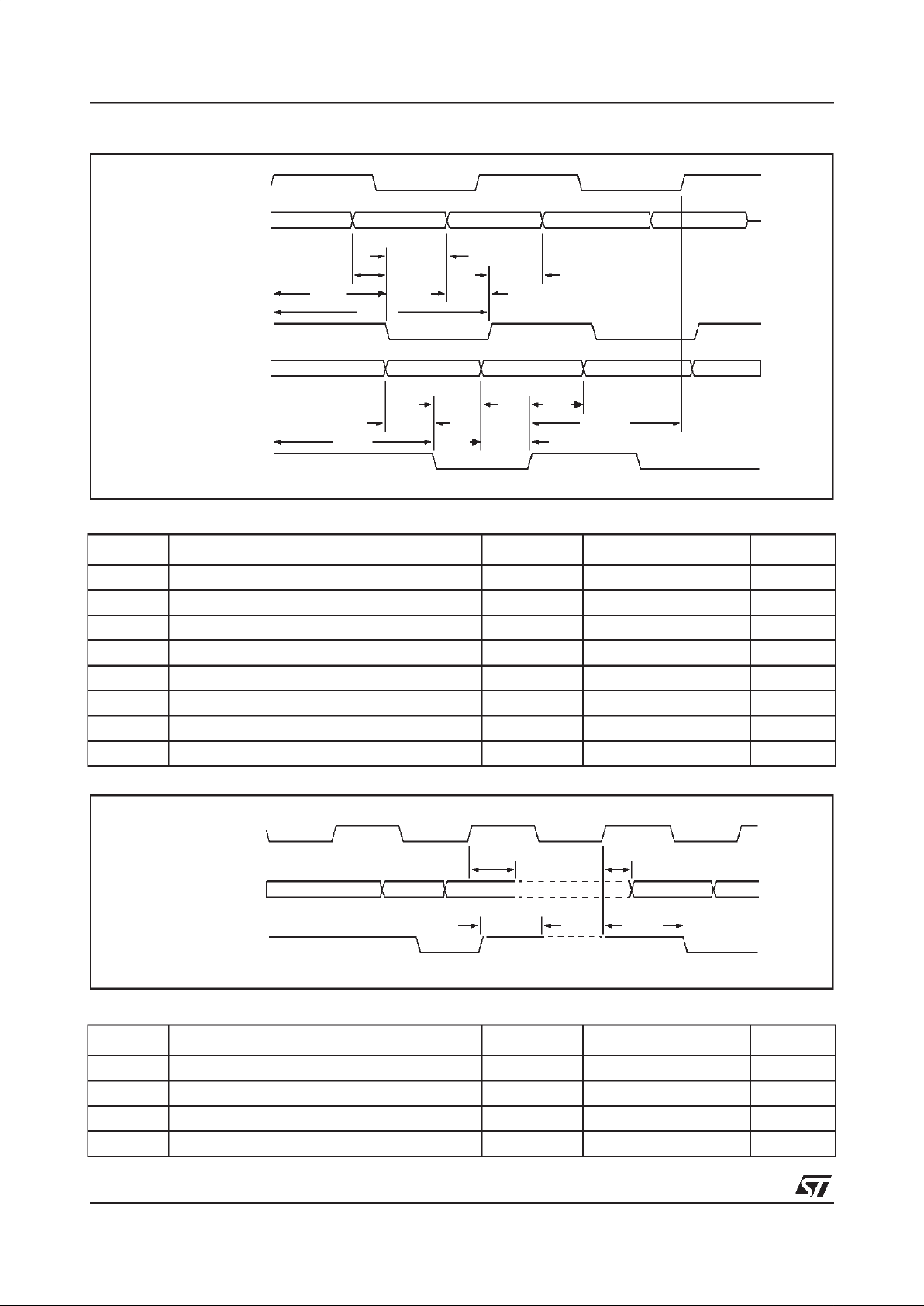
Figure 14. AGP timing diagram (2X data transfer mode)
Table 3. AGP timing parameters (2X data transfer mode)
Figure 15. AGP Strobe/Data turnaround timing diagram (2X data transfer mode)
Table 4. AGP Strobe/Data turnaround timing parameters (2X data transfer mode)
Symbol Parameter Min. Max. Unit Notes
t
TSF AGPCLK to transmit strobe falling edge 2 12 ns
t
TSR AGPCLK to transmit strobe rising edge 20 ns
t
DVB Output data validbefore strobe 1.7 ns
t
DVA Output data validafter strobe 1.7 ns
t
RSSU Receiver strobe setup time to AGPCLK 6ns
t
RSH Receiver strobe hold time from AGPCLK 1ns
t
DSU Input data to strobe setup time 1 ns
t
DH Input data to strobe hold time 1 ns
Symbol Parameter Min. Max. Unit Notes
t
OND Float to active delay -1 9 ns
t
OFFD Active to float delay 1 12 ns
t
ONS Strobe active to strobe falling edge setup 6 10 ns
t
OS Strobe rising edge to strobe float delay 6 10 ns
t
DVB
tDVA
tTSF
tDVB
tDVA
tTSR
tRSH
tDSU
tDH
tDSU
tDH
tRSSU
Data1 Data2 Data3 Data4
Data1 Data2 Data3 Data4
AGPCLK
Output data
Output strobe
Input data
Input strobe
t
OFFS
tOFFD tOND
tONS
AGPCLK
PCIAD[31:0]
AGPADSTBx

128-BIT 3D MULTIMEDIA ACCELERATOR RIVA128ZX
23/85
5 PCI 2.1 LOCAL BUS INTERFACE
5.1 RIVA128ZX PCI INTERFACE
The RIVA128ZXsupports a gluelessinterface to PCI 2.1 with both master andslave capabilities. Thehost
interface is fully compliant with the 32-bit PCI 2.1 specification.
The Multimedia Accelerator supports PCI bus operation up to 33MHz with zero-wait state capability and
full bus mastering capability handling burst reads and burst writes.
Figure 16. PCI interface pin connections
Table 5. PCI bus commands supported by the RIVA128ZX
Bus master Bus slave
Memory read and write Memory read and write
Memory read line I/O read and write
Memory read multiple Configuration read and write
Memory read line
Memory read multiple
Memory write invalidate
PCI bus
PCICBE[3:0]#
PCIAD[31:0]
PCIFRAME#
32
4
PCIDEVSEL#
PCIIRDY#
PCITRDY#
PCISTOP#
PCIIDSEL
PCIREQ#
PCIGNT#
PCICLK
PCIRST#
PCIPAR
PCIINTA#
RIVA128ZX

128-BIT 3D MULTIMEDIA ACCELERATORRIVA128ZX
24/85
5.2 PCI TIMING SPECIFICATION
The timing specification of the PCIinterface takes the form of generic setup, hold and delay times of tran-
sitions to and from the rising edge of PCICLK as shown in Figure 17.
Figure 17. PCI timing parameters
Table 6. PCI timing parameters
NOTE
1 PCIREQ# and PCIGNT# are point to point signals andhave different valid delay and input setup times than bussed sig-
nals. All other signals are bussed.
Symbol Parameter Min. Max. Unit Notes
t
VAL PCICLK to signal valid delay (bussed signals) 2 11 ns 1
t
VAL
(PTP)
PCICLK to signal valid delay (point to point) 2 12 ns 1
t
ON Float to activedelay 2 ns
t
OFF Active to float delay 28 ns
t
SU Inputset up time to PCICLK (bussed signals) 7 ns 1
t
SU
(PTP)
Input set up time to PCICLK (PCIGNT#)10 ns1
t
SU
(PTP)
Input set up time to PCICLK (PCIREQ#)12 ns
t
H Input hold time fromPCICLK 0ns
t
VAL
tON
tOFF
tSU tH
PCICLK
Output delay
Tri-state output
Input
PCICLK
Output timing parameters
Input timing parameters
128-BIT 3D MULTIMEDIA ACCELERATOR RIVA128ZX
25/85
Figure 18. PCI Target write - Slave Write (single 32-bit with 1-cycle DEVSEL# response)
Figure 19. PCI Target write - Slave Write (multiple 32-bit with zero wait state DEVSEL# response)
address data
bus cmd BE[3:0]#
(med)
PCICLK
PCIAD[31:0]
PCICBE[3:0]#
PCIFRAME#
PCIIRDY#
PCITRDY#
PCIDEVSEL#
address data0
bus cmd BE[3:0]#
data1 data2
BE[3:0]# BE[3:0]#
PCICLK
PCIAD[31:0]
PCICBE[3:0]#
PCIFRAME#
PCIIRDY#
PCITRDY#
PCIDEVSEL#
128-BIT 3D MULTIMEDIA ACCELERATORRIVA128ZX
26/85
Figure 20. PCI Target read - Slave Read (1-cycle single word read)
Figure 21. PCI Target read - Slave Read (slow single word read)
address
bus cmd BE[3:0]#
data0
PCICLK
PCIAD[31:0]
PCICBE[3:0]#
PCIFRAME#
PCIIRDY#
PCITRDY#
PCIDEVSEL#
address
bus cmd BE[3:0]#
data0
PCICLK
PCIAD[31:0]
PCICBE[3:0]#
PCIFRAME#
PCIIRDY#
PCITRDY#
PCIDEVSEL#
 Loading...