

SGS Thomson Microelectronics STG3000X Datasheet
RIVA 128™
128-BIT 3D MULTIMEDIA ACCELERATOR
™
1/77
The information in this datash eet is subject to change
42 1687 01 (SGS-THOMSON)
October 1997
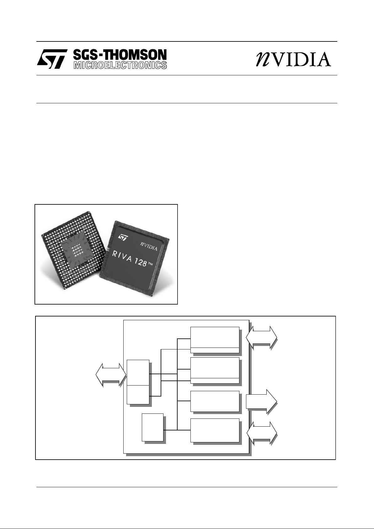
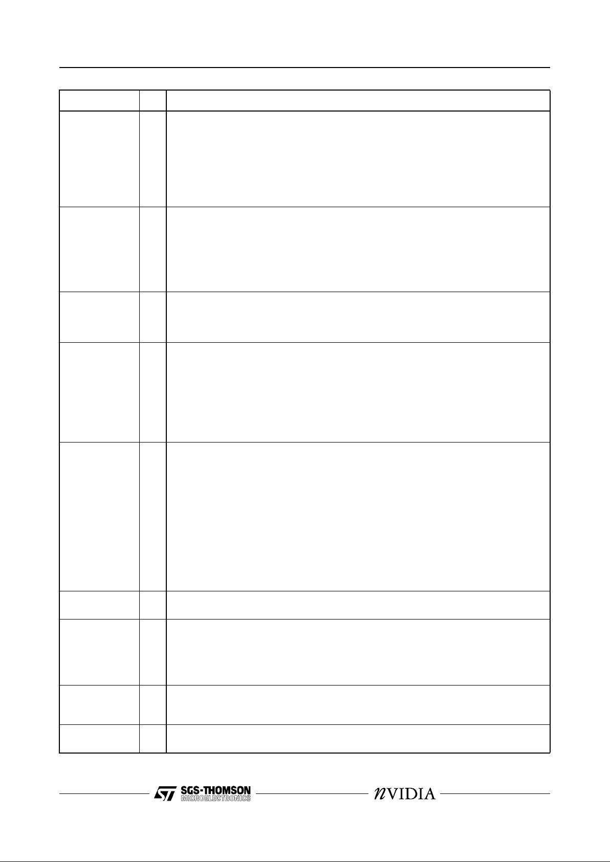
BLOCK DIAGRAM
Palette DAC
YUV - RGB,
Graphic s E ng i ne
128 bit 2D
Direct3D
SGRAM Interface
VGA
DMA Bus
Internal Bus
CCIR656
Video
PCI/AGP
128 bit
interface
Monitor/
TV
1.6 GByte/s
Internal Bus
Bandwidth
DMA Engine
Video Port
X & Y scaler
Host
Interface
FIFO/
DMA
Pusher
DMA Engine
DESCRIPTION
The RIVA 128™ is the first 128-bit 3D Multimedia
Accelerator to offer unparalleled 2D and 3D performance, meeting all the r equirements of the mainstream PC graphics market and Microsoft’s
PC’97. The RIVA 128 introduces the most advanced Direct3D™ acceleration solution and also
delivers leadership VGA, 2D and Video performance, enabling a range of applications from 3D
games through to DVD, Intercast™ and video conferencing.
KEY FEATURES
•
Fast 32-bit VGA/SVGA
•
High performance 128-bit 2D/GUI/DirectDraw
Acceleration
•
Interactive, Photorealistic Direct3D Acceleration with advanced effects
•
Massive 1.6Gbytes/s, 100MHz 128-bit wide
frame buffer interface
•
Video Acceleration for DirectDraw/DirectVideo,
MPEG-1/2 and Indeo
®
- Planar 4:2:0 and packed 4:2:2 Color Space
Conversion
- X and Y smooth up and down scaling
•
230MHz Palette-DAC supporting up to
1600x1200@75Hz
•
NTSC and PAL output with flicker-filter
•
Multi-function Video Port and serial interface
•
Bus mastering DMA 66MHz Accelerated
Graphics Port (AGP) 1.0 Interface
•
Bus mastering DMA PCI 2.1 interface
•
0.35 micron 5LM CMOS
•
300 PBGA

RIVA 128 128-BIT 3D MULTIMEDIA ACCELERATOR
TABLE OF CONTENTS
2/77
1 REVISION HISTORY...................................................................................................................... 4
1 RIVA 128 300PBGA DEVICE PINOUT.......................................................................................... 5
2 PIN DESCRIPTIONS...................................................................................................................... 6
2.1 ACCELERATED GRAPHICS PORT (AGP) INTERFACE..................................................... 6
2.2 PCI 2.1 LOCAL BUS INTERFACE........................................................................................ 6
2.3 SGRAM FRAMEBUFFER INTERFACE................................................................................ 8
2.4 VIDEO PORT......................................................................................................................... 8
2.5 DEVICE ENABLE SIGN ALS... ... .................................................... ... ..................................... 9
2.6 DISPLAY INTERFACE.......................................................................................................... 9
2.7 VIDEO DAC AND PLL ANALOG SIGNALS.......................................................................... 9
2.8 POWER SUPPLY.................................................................................................................. 9
2.9 TEST...................................................................................................................................... 10
3 OVERVIEW OF THE RIVA 128...................................................................................................... 11
3.1 BALANCED PC SYSTEM...................................................................................................... 11
3.2 HOST INTERFACE ...............................................................................................................11
3.3 2D ACCELERATION................. .... .............................. .... ...................................................... 12
3.4 3D ENGINE..................... ............................... ... .................................................................... 12
3.5 VIDEO PROCESSOR............................................................................................................ 12
3.6 VIDEO PORT......................................................................................................................... 13
3.7 DIRECT RGB OUTPUT TO LOW COST PAL /NT SC ENC ODER........... ... ..................... ... ... 13
3.8 SUPPORT FOR STANDAR D S...... ... ................................................... .... .............................. 13
3.9 RESOLUTIONS SUPPORTED.............................................................................................. 13
3.10 CUSTOMER EVALUATION KIT ............................................................................................ 14
3.11 TURNKEY MANUFACTURING PACKAGE........................................................................... 14
4 ACCELERATED GRAPHICS PORT (AGP) INTERFACE............................................................. 15
4.1 RIVA 128 AGP INTERFACE................................................................................................. 1 6
4.2 AGP BUS TRANSACTIONS.................................................................................................. 1 6
5 PCI 2.1 LOCAL BUS INTERFACE................................................................................................. 2 2
5.1 RIVA 128 PCI INTERFACE................................................................................................... 22
5.2 PCI TIMING SPECIFICATION............................................................................................... 23
6 SGRAM FRAMEBUFF E R INTERFA C E........... ................................................... .... ....................... 29
6.1 SGRAM INITIALIZATION...................................................................................................... 31
6.2 SGRAM MODE REGISTER.................................................................................................. 31
6.3 LAYOUT OF FRAMEBUFFER CLOCK SIGNALS................................................................ 32
6.4 SGRAM INTERFACE TIMING SPECIFICATION.................................................................. 32
7 VIDEO PLAYBACK ARCHITECTURE........................................................................................... 37
7.1 VIDEO SCALER PIPELINE ................................................................................................... 38
8 VIDEO PORT.................................................................................................................................. 40
8.1 VIDEO INTERFACE PORT FEATURES............................................................................... 40
8.2 BI-DIRECTIONAL MEDIA PORT POLLING COMMANDS USING MPC.............................. 41
8.3 TIMING DIAGRAMS..............................................................................................................42
8.4 656 MASTER MODE............................................................................................................. 46
8.5 VBI HANDLING IN THE VIDEO PORT................................................................................. 47
8.6 SCALING IN THE VIDEO PORT.............................. ... .......................................................... 47
9 BOOT ROM INTERFACE......... ................................................... .... ............................................... 48

128-BIT 3D MULTIMEDIA ACCELERATOR RIVA 128
3/77
10 POWER-ON RESET CONFIGURATION........................................................................................ 50
11 DISPLAY INTERFACE................................................................................................................... 52
11.1 PALETTE-DAC...................................................................................................................... 52
11.2 PIXEL MODES SUPPORTED ............................................................................................... 52
11.3 HARDWARE CURSO R.......... ............................................................. .... .............................. 53
11.4 I2C INTERFACE.................................................................................................................... 54
11.5 ANALOG INTERFACE.......................................................................................................... 55
11.6 TV OUTPUT SUPPORT...................................................................... .... .............................. 56
12 IN-CIRCUIT BOARD TESTING......................................................................................................58
12.1 TEST MODES............................................................................... ... ..................................... 58
12.2 CHECKSUM TEST................................................................................................................ 58
13 ELECTRICAL SPEC IF ICA TI ONS.................................. ... ............................................................. 59
13.1 ABSOLUTE MAXIMUM RATINGS............. ................................... ........................................ 59
13.2 OPERATING CONDITIONS.................................................................................................. 59
13.3 DC SPECIFICATI ON S..... ... ............................... .... ............................................................. .. .59
13.4 ELECTRICA L SPECIFICATIONS.......................... ... ................................................... .... ...... 60
13.5 DAC CHARACTERISTICS.................................................................................................... 60
13.6 FREQUENCY SYNTHESIS CHARACTERISTICS................................................................ 61
14 PACKAGE DIMENSION SPECIFICATION.................................................................................... 62
14.1 300 PIN BALL GRID ARRAY PACKAGE.............................................................................. 62
15 REFERENCES................................................................................................................................ 63
16 ORDERING INFORMATION..........................................................................................................63
APPENDIX...................................................................................................................................... 64
A PCI CONFIGURATION REGISTERS............................................................................................. 64
A.1 REGISTER DESCRIPTIONS FOR PCI CONFIGURATION SPACE.................................... 64
128-BIT 3D MULTIMEDIA ACCELERATORRIVA 128
4/77
1 REVISION HISTORY
Date Section, page Descripti on of change
15 Jul 97 6, page 28 Updat e of SG R AM fram ebuf fer int er face conf ig ura ti on di agrams.
28 Aug 97 13.5, page 59 Change of DAC specification from 206MHz to 230M Hz max. oper ating frequency.
29 Aug 97 6.3, page 31 Updat e t o re com mendation for connect ion of
FBCLK2
and
FBCLKB
pins.
4 Sep 97 10, page 49 Update to RAM Type Power-On Reset confi gur ation bits.
15 Sep 97 13, page 58 Temperature specificat ion TC now based on case, not ambient temperature.
15 Sep 97 13, page 58 Change to Power Supply voltage VDD specification.
17 Sep 97 1, page 5 Change to Video Port pin nam es.
17 Sep 97 2, page 6 Chang e to Vid eo Port pin descr iptions.
17 Sep 97 8, page 39 Updates to Video Port section.
18 Sep 97 11.6, page 55 Change to capacitor value in TV output implementation schematic.
18 Sep 97 13.3, page 58 Change to power dissipation specifi cat ion.
25 Sep 97 4.2, page 16 Rem oval of AGP flow control descriptio n.
25 Sep 97 11.4, page 53 Updates to Ser ial Port descrip tion.
128-BIT 3D MULTIMEDIA ACCELERATOR RIVA 128
5/77
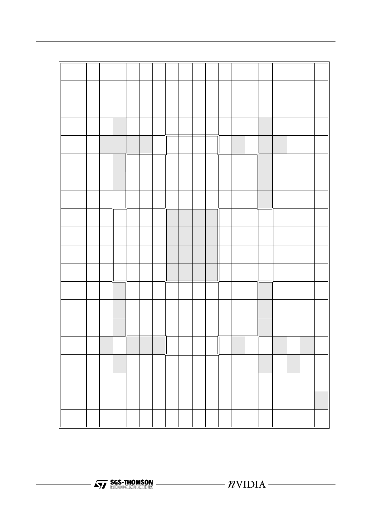
1 RIVA 128 300PBGA DEVICE PINOUT
NOTES
1 NIC = No Internal Connection. Do not connect to these pins.
2 VDD=3.3V
∗
Signals denoted with an asterisk are defined for future expansi on. See
Pin Descriptions
, Section 2, page 6 for details.
1234567891011121314151617181920
A
FBD[4] FBD[6] FBD[7] FBD[17] FBD[19] FBD[21] FBD[23] FBDQM[2] FBA[0] FBA[2] FBA[4] FBA[6] FBA[8] FBDQM[5] FBD[41] FBD[43] FBD[45] FBD[47] FBD[56] FBD[57]BFBD[3] FBD[5] FBD[16] FBD[18] FBD[20] FBD[22] FBDQM[0] FBA[9] FBA[1] FBA[3] FBA[5] FBA[7] FBCLK1 FBDQM[7] FBD[40] FBD[42] FBD[44] FBD[46] FBD[58] FBD[59]CFBD[1] FBD[2] FBD[28] FBD[27] FBD[26] FBD[25] FBD[15] FBD[13] FBD[11] FBD[9] FBDQM[1] FBWE# FBRAS#
FBA[10]
∗
FBDQM[4] FBD[55] FBD[54] FBD[53] FBD[60] FBD[61]
D
FBCLK0 FBD[0] FBD[29] FBD[30] VDD FBD[24] FBD[14] FBD[12] FBD[10] FBD[8] FBDQM[3] FBCAS# FBCS0 FBCS1 FBDQM[6] VDD FBD[52] FBD[51] FBD[62] FBD[63]
E
SCL FBCLK2 FBD[31] VDD NIC VDD VDD VDD
FBCKE
∗
VDD VDD VDD VDD FBD[50] FBD[39] FBD[38]
F
MP_AD[6] NIC SDA FBCLK FB VDD VDD FBD[48] FBD[49] FBD[37] FBD[36]
G
MPFRAME# MP_AD[7] MP_AD[5] MP_AD[4] MPCLAMP VDD FBD[35] FBD[34] FBD[33] FBD[32]
H
MP_AD[2] MPSTOP# MPCLK M P_AD[3] VDD NIC FBDQM[12] FBDQM[14] FBDQM[15] FBDQM[13]
J
FBDQM[8] MPDTACK# MP_AD[1] MP_AD[0] GND GND GND GND FBD[118] FBD[119] FBD[105] FBD[104]KFBDQM[9] FBD[87] FBDQM[10] FBDQM[11] GND GND GND GND FBD[116] FBD[117] FBD[107] FBD[106]
L
FBD[86] FBD[85] FBD[72] FBD[73] GND GND GND GND FBD[114] FBD[115] FBD[109] FBD[108]MFBD[84] FBD[83] FBD[74] FBD[75] GND GND GND GND FBD[112] FBD[113] FBD[111] FBD[110]NFBD[82] FBD[81] FBD[76] FBD[77] NIC NIC FBD[102] FBD[103] FBD[121] FBD[120]PFBD[80] FBD[71] FBD[78] FBD[79] VDD VDD FBD[100] FBD[101] FBD[123] FBD[122]RFBD[70] FBD[69] FBD[88] FBD[89] NIC NIC FBD[98] FBD[99] FBD[125] FBD[124]
T
FBD[68] FBD[67] FBD[90] VDD NIC HOSTVDD HO ST VDD
HOST-
CLAMP
HOSTVDD
HOST-
CLAMP
HOSTVDD
HOST-
CLAMP
VDD FBD[97] FBD[127] FBD[126]
U
FBD[66] FBD[65] FBD[92] FBD[91]
HOST-
CLAMP
XTALOUT PCIRST# AGPST[1] PCIAD[30] PCIAD[26] PCICBE# [3] PCIAD[20 ] PCIAD[16] PCITRDY# PCIPAR
HOSTVDD PCICBE#[0] FBD[96] VIDVSYNC VIDHSYNC
V
FBD[64] FBD[95] RED DACVDD VREF PCIINTA# PCIGNT# AGPPIPE# PCIAD[28] PCIAD[24] PCIAD[22] PCIAD[18] PCIFRAME# PCISTOP# PCIAD[15] PCIAD[11] PCIAD[6] PCIAD[2] TESTMODEROMCS#WFBD[93] FBD[94] BLUE COMP PLLVDD PCIREQ# AGPST[2] PCIAD[31] PCIAD[27]
AGPAD-
STB1
∗
PCIAD[21] PCIAD[17] PCIIRDY# PCICBE#[1] PC IAD[ 13] PCIAD[9] PCIAD[4] PCIAD[0] PCIAD[7] PCIAD[5]
Y
GREEN GND R SET XTALIN PCICLK AGPST[0]
PCIIDSEL/
AGPRBF#
PCIAD[29] PCIAD[25] PCIAD[23] PCIAD[19] PCICBE#[2 ]
PCI-
DEVSEL#
PCIAD[14] PCIAD[12] PCIAD[10] PCIAD[8]
AGPAD-
STB0
∗
PCIAD[3] PCIAD[1 ]
128-BIT 3D MULTIMEDIA ACCELERATORRIVA 128
6/77
2 PIN DESCRIPTIONS
2.1 ACCELERATED GRAPHICS PORT (AGP) INTERFACE
2.2 PCI 2.1 LOCAL BUS INTERFACE
Signal I/O Description
AGPST[2:0]
I AGP status bus providing information from the arbiter to the RIVA 128 on what it may do.
AGPST[2:0]
only have meaning to the RIVA 128 when
PCIGNT#
is asserted. W hen
PCIGNT#
is de-asser t ed t hese signals have no meaning and must be ignore d.
000 Indicate s tha t previously requested low priority read or flush data is being
returned to the RIVA 128.
001 Indica te s tha t previously requested hi gh priority r ead data is being ret urned to
the RIVA 128.
010 Indica te s tha t the RIVA 128 is to provide low priority write data for a previous
enqueued wr it e com m and.
011 Indicates that the RIVA 128 is to provide high priority write data for a previous
enqueued wr it e com m and.
100 Reserved
101 Reserved
110 Reserved
111 Indicate s tha t the RIVA 128 has been given permission to sta rt a bus transac-
tion. The RIVA 128 may enqueue AGP requests by asserting
AGPP IPE#
or sta rt
a PCI transaction by asserting
PCIFRAME#. AGPST[2:0]
are always an output
from the Core Logic (AGP chipset) and an input to the RIVA 128.
AGPRBF#
O Read Buffer Full indicates when the RIVA 128 is ready to accept previously requested low
priority read data or not. When
AGPRBF#
is assert ed t he ar biter is not allowed to return
(low priority) read data to the RIVA 128. This signal should be pulled up via a 4.7KΩ resistor (although it is supposed to be pull ed up by the motherboard chipset).
AGPPIPE#
O Pipel ine d Re ad is asserted by RIVA 128 (when the current master) to indicat e a full w id th
read address is to be enqu eued by the target. The RI VA 128 enqueues one requ est each
rising clock edge while
AGPPIPE#
is assert ed. When
AGPPIPE#
is de-asserted no new
requests are enqueued across
PCIAD[31:0]. AGPPIPE#
is a sustained tri-state signal
from the RIVA 128 and is an input to the target (the core logic).
AGPADSTB0
∗,
AGPADSTB1
∗
I/O These signals are currently a “no-connect” in this revision of the RIVA 128 but may be acti-
vated to support AGP double-edge clocking in future pin compatible devices. It is recommended that thes e pins are connected directly to the AD _S TB0 and AD_STB1 pins
defined in the AGP specification.
Signal I/O Descripti on
PCICLK
I PCI clock. This si gnal pr ovides timing for all transaction s on th e PC I bus, except for
PCIRST#
and
PCIINTA#
. All PCI signals are sampl ed on the rising edge of
PCICLK
and
all timing parameters are defined with respect to this edge.
PCIRST#
I PCI reset. This signal is used to bring registers, sequencers and signals to a consistent
state. When
PCIRST#
is asserted all output signals are t r istated.
PCIAD[31:0]
I/O 32-bit multiplexed address and data bus. A bus transaction cons ists of an address phase
followed by one or more data phases.
128-BIT 3D MULTIMEDIA ACCELERATOR RIVA 128
7/77
PCICBE[3:0]#
I/O Multiplexed bus command and byte enable signals. During t he address phase of a trans-
action
PCICBE[3:0]#
define the bus command, during the dat a phase
PCICBE[3:0]#
are
used as byte enables. The byte enables are valid for the entire data phase and determine
which byte lanes contain valid data.
PCICBE[0]#
applies to byte 0 (LSB) and
PCICBE[3]#
applies to byte 3 (MSB).
When connected to AGP these signals carry different commands than PCI when requests
are being enqueued using
AGPPIPE#
. Valid byte information is provided during AGP write
transactions.
PCICBE[3:0]#
are not used during the return of AGP read data.
PCIPAR
I/O Parity. Th is si gnal is the even parity bit generated acr oss
PCIAD[31:0]
and
PCICBE[3:0]#. PCIPAR
is stable and valid one clock after the address phase. For data
phases
PCIPAR
is stable and valid one clock after either
PCIIRDY#
is asserted on a write
transaction or
PCITRDY#
is asserted on a r ead transaction. Once
PCIPAR
is valid, it
remains valid until one clock after completion of the current data phase. The master drives
PCIPAR
for address and write data phases; the target drives
PCIPAR
for read data
phases.
PCIFRAME#
I/O Cycle frame. This signal is driven by the current master to indicate the beginning of an
access and its duration.
PCIFRAME#
is asserted to indi cat e t hat a bus transact ion is
beginning. Dat a transfers continue while
PCIFRAME#
is assert ed. When
PCIFRAME#
is
deassert ed, the transactio n is in the final data phase.
PCIIRDY#
I/O Initiator ready. This signal indicates the initiator’s (bus master’s) ability to complete the cur-
rent data phase of the tran sact ion. See extended descri pt ion for
PCITRDY#
.
When connected to AGP this signal indicates the initiator (AGP compliant master) is ready
to provide all write data for the current transaction. Once
PCIIRDY#
is asserted for a write
operation, the master is not allowed to insert wait states. The assertion of
PCIIRDY#
for
reads, indicates that the ma ste r is re ady to transfer a subsequent block of read data. The
master is never allowed to insert a wait state during the initial block of a read t rans act io n.
However, it may ins ert wa it states after ea c h bl o ck trans fers.
PCITRDY#
I/O Target rea dy. This signal indicates the tar get ’s (selecte d device’s) ability to compl et e th e
current data phase of the transaction.
PCITRDY#
is used in conjunction with
PCIIRDY#
. A data phase is completed on any clock
when both
PCITRDY#
and
PCIIRDY#
are sampled as being asser te d. During a read,
PCITRDY#
indicates that valid data is present on
PCIAD[31:0]
. During a write, it in dica tes
the target is prepared to accept data. Wait cycles are inserted until bot h
PCIIRDY#
and
PCITRDY#
are asser t ed together.
When connected to AGP this signal indicates the AGP compliant target is ready to provide
read data for the entire transact ion (when transaction can complete with in four clocks) or
is ready to transfer a (initial or subsequent) block of data, when the transfer requires more
than four clocks to complete. The target is al lowed to insert wait states af t er each block
transfers on both read and write transactions.
PCISTOP#
I/O
PCISTOP#
indicates that the current target is requesting the master to terminate the cur-
rent transaction.
PCIIDSEL
I Initializ at ion device select. This signa l is used as a chip select during configuration read
and write transacti ons.
For AGP applications note that ID S EL i s not a pin on the AGP connector. The RIVA 128
performs the device select de code internally within its host interface. It is not required to
connect the AD16 signal to the IDSEL pin as suggested in the AGP specifica tion.
PCIDEVSEL#
I/O Device select. When acting as an output
PCIDEVSEL#
indicates that the RIVA 128 has
decoded the PCI address and is claimin g the cur re nt access as the target. As an input
PCIDEVSEL#
indicates w hethe r any ot her de vice on t he bu s ha s been se l ecte d .
PCIREQ#
O Request. This signal is asserted by the RIVA 128 to indicate to the arbiter that it desires to
become master of the bus.
Signal I/O Description
128-BIT 3D MULTIMEDIA ACCELERATORRIVA 128
8/77
2.3 SGRAM FRAMEBUFFER INTERFACE
2.4 VIDEO PORT
PCIGNT#
I Grant. This sign al i ndi cat es to the RI VA 128 that access to the bus has bee n granted and
it can now become bus master.
When connected to AGP additional information is provided on
AGPST[2:0]
indicating that
the master is the recipient of previously requested read data (high or low priority), it is to
provide write dat a (h igh or low priorit y ), for a previous ly en queued write command or has
been given permis sion to start a bus transaction (AGP or PCI).
PCIINTA#
O Interrupt reques t line. This open drain output is asserted and deasserted async hronously
to
PCICLK
.
Signal I/O Descripti on
FBD[127:0]
I/O The 128-bit SGRAM memory data bus.
FBD[31:0]
are also used to access up to 64KBytes of 8-bit ROM or Fla sh ROM, using
FBD[15:0]
as address ROMA[15 :0 ],
FBD[31:2 4]
as ROMD[7:0],
FBD[17]
as ROMWE#
and
FBD[16]
as ROMOE#.
FBA[10:0]
O Memory Address bus. Conf igu ratio n st rap pin g options are also deco ded on these signals
during PCIRST# as descri bed i n Section 10, page 49.
[FBA[10]
is reserved for future
expansion and should be pu ll ed t o
GND
via a 4.7KΩ resistor.
FBRAS#
O Memory Row Address Strobe for all memory devices.
FBCAS#
O Memory Column Address Strobe for all memory devices.
FBCS[1:0]#
O Memory Chip Select strobes for each SGRAM bank.
FBWE#
O Memory Write Enable strobe for all memory devices.
FBDQM[15:0]
O Memory Data/Output Enable strobes for each of the 16 bytes.
FBCLK0,
FBCLK1,
FBCLK2
O Memory Clock signals. Sepa rate cl ock signals
FBCLK0
and
FBCLK1
are pr ovided fo r
each bank of SGRAM for reduced clock skew and loading.
FBCLK2
is fed back to
FBCLKFB
. Details of recommended memor y cl ock layout are given in Sect ion 6.3 , pag e
31.
FBCLKFB
I Framebuffer clock feedback.
FBCLK2
is fed back to
FBCLKFB
.
FBCKE
∗ O This signal is currently a “no-connect” in this revision of the RIVA 128 but may be activated
to support the framebuffer memory clock enable for power management in future pin compatible devices. It is recommended that this pin is tied t o VD D t hr ough a 4.7KΩ pull-up
resistor.
Signal I/O Description
MP_AD[7:0]
I/O Media Port 8-bit multiplexed address and data bus or ITU- R- 656 video data bus when in
656 mode.
MPCLK
I 40MHz Me di a Por t sys tem cl ock or pixel clock when in 65 6 m ode.
MPDTACK#
I Media Port data transfer acknowledgment signal.
MPFRAME#
O Initiates Media Port transfers when ac tive, ter m inates transfers when inactive.
MPSTOP#
I Media Port control signal used by the slave to terminate transfers.
Signal I/O Description
128-BIT 3D MULTIMEDIA ACCELERATOR RIVA 128
9/77
2.5 DEVICE ENABLE SIGNALS
2.6 DISPLAY INTERFACE
2.7 VIDEO DAC AND PLL ANALOG SIGNALS
2.8 POWER SUPPLY
Signal I/O Description
ROMCS#
O Enables reads from an external 64Kx 8 or 32Kx8 ROM or Flash ROM. Thi s signal is used
in conjunction with framebuffer data lines as described above in Section 2.3.
Signal I/O Descripti on
SDA
I/O Used for DDC2B+ monitor communica ti on and interface to video decoder devices.
SCL
I/O Used for DDC2B+ monitor communica ti on and interface to video decoder devices.
VIDVSYNC
O Vertical sync supplied to the display monitor. No buffering is required. In TV mode this sig-
nal supplies composite sync to an externa l PAL/NTSC encoder.
VIDHSYNC
O Hor izon tal sync supplied to the displ ay monito r. No buffering is required .
Signal I/O Descripti on
RED,
GREEN,
BLUE
O RGB display moni t or out puts. These are softwar e configurable to drive eith er a doubly ter -
minated or singly terminated 75Ω load.
COMP
- Externa l compensation capacitor for the video DACs. This pin should be connected to
DACVDD
via the compensat io n capacitor, see Figure 58, page 54 .
RSET
- A precision resis to r placed between this pin and GND sets the full-scal e video DAC current, see Figure 58, page 54.
VREF
- A capacitor sho uld be placed between thi s pin and GND as shown in Figure 58, page 54.
XTALIN
I A series resonant crystal is connected between these two points to provide the reference
clock for the internal MCLK and VCLK clock synthesizers, see Figu re 58 and Table 16,
page 54. Alternately, an external L V TTL clock oscillator output may be driven into
XTA-
LOUT
, connecting
XTALIN
to GND. For designs supporting TV-out,
XTALOUT
should be
driven by a reference clock as described in Se ct ion 11.6, page 55.
XTALOUT
O
Signal I/O Descripti on
DACVDD
P Analog power supply for the video DACs.
PLLVDD
P Analog power supply for all clock synthesizers.
VDD
P Digital power supply.
GND
P Ground.
MPCLAMP
P
MPCLAMP
is connected to +5V to protect the 3.3V RIVA 128 from external devices which
will potentially dr ive 5V signal levels onto the Video Port in put pin s.
HOSTVDD
P
HOSTVDD
is connected to the Vddq 3. 3 pins on the AGP connector. This is the supply
voltage for the I/O buffers and is isolated from the core VD D. On AGP designs these pins
are also connect ed t o the
HOSTCLAMP
pins. On PCI designs they are con nected to the
3.3V supply.
HOSTCLAMP
P
HOSTCLAMP
is the supply signalling rail protection for the host interface. In AGP designs
these signals are con nected to Vddq 3.3. For PCI desig ns th ey are co nnected to the I/O
power pins (V
(I/O)
).
128-BIT 3D MULTIMEDIA ACCELERATORRIVA 128
10/77
2.9 TEST
Signal I/O Description
TESTMODE
I For designs which wi ll be t est ed in -circuit, this pin sho uld be connected to GND throu gh a
10KΩ pull-down resi sto r, otherwise this pin should be conne cte d directly to GND. When
TESTMODE
is asser te d,
MP_AD[3:0]
are reassigned as
TESTCTL[ 3:0]
respectively.
Information on in -c ircuit test is given in Section 12, page 57.

128-BIT 3D MULTIMEDIA ACCELERATOR RIVA 128
11/77
3 OVERVIEW OF THE RIVA 128
The RIVA 128 is the first 128-bit 3D Mu ltimedia
Accelerator to offer unparalleled 2D and 3D performance, meeting all the requirements of the mainstream PC graphics market and Microsoft’s
PC’97. The RIVA 128 introduces the most advanced Direct3D™ accelera tion solution and al so
delivers leadership VGA, 2D and Video performance, enabling a range of applications from 3D
games through to DVD, Intercast™ and video conferencing.
3.1 BALANCED PC SYSTEM
The RIVA 128 is designed to leverage existing PC
system resources such as system memory, high
bandwidth internal buses and bus master capabilities. The synergy between the RIVA 128 graphics
pipeline architecture and that of the current generation PCI and next generation AGP platforms, defines ground breaking performance levels at the
cost point currently required for mainstream PC
graphics solutions.
Execute versus DMA models
The RIVA 128 is architected to optimize PC system resources in a manner consistent with the
AGP “Execute” model
. In this model texture map
data for 3D applications is stored in system memory and individual texels are accessed as needed
by the graphics pipeline. This is a significant enhancement over the DMA model where entire texture maps are transferred into off-screen framebuffer memory.
The advantages of the Execute versus the DMA
model are:
•
Improved system performance since only the
required texels and not the e ntire texture ma p,
cross the bus.
•
Substantial cost savings since all the framebuffer is usable for the displayed screen and Z buffer and no part of it i s required to b e dedicated
to texture storage or texture caching.
•
There is no software overhead in the Direct3D
driver to manage texture caching between application memory and the framebuffer.
To extend the advantages of the Execute model,
the RIVA 128’s proprietary tex ture cache and virtual DMA bus master design overcomes the bandwidth limitation of PCI, by sustaining a hi gh texel
throughput with minimum bus utilization. The host
interface supports burst transactions up to 66MHz
and provides over 200MBytes/s on AGP. AGP ac-
cesses offer other performance enhancements
since they are from non-cacheable memory (no
snoop) and can be low priority to prevent processor stalls, or high priority to prevent graphics engine stalls.
Building a balanced system
RIVA 128 is architected to provide the level of 3D
graphics performance and quality available in top
arcade platforms. To provide comparable scene
complexity in the 1997 time-frame, processors will
have to achieve new levels of floating point performance. Profiles have shown that 1997 mainstream CPUs will be ab le to transform ove r 1 million lit, meshed triangles/s at 50% utilization using
Direct3D. This represents an order of magnitude
performance increase over anything attainable in
1996 PC games.
To build a balanced system the gr aphics pipeline
must match the CPU’s performance. It must be capable of rendering at least 1 million polygons/s in
order to avoid CPU stalls. Factors affecting this
system balance include:
•
Direct3D compatibility. Minimizing the differences between the hardware interface and the
Direct3D data structures.
•
Triangle setup. Minimizing the number of format conversions and delta calculations done by
the CPU.
•
Display-list processing. Avoiding CPU stalls by
allowing the graphics pipeline to execute independently of the CPU.
•
Vertex caching. Avoids saturating the host interface with repeated vertices, lowering the traffic on the bus and reducing system memory collisions.
•
Host interface performance.
3.2 HOST INTERFACE
The host interface boosts communication between
the host CPU and the RIVA 128. The optimized interface performs burst DMA bus mastering for efficient and fast data transfer.
•
32-bit PCI version 2.1 or AGP version 1.0
•
Burst DMA Master and target
•
33MHz PCI clock rate or 66MHz AGP clock rate
•
Supports over 100MBytes/s with 33MHz PCI
and over 200MBytes/s on 66MHz AGP
•
Implements read buffer posting on AGP
•
Fully supports the “Execute” model on both PCI
and AGP

128-BIT 3D MULTIMEDIA ACCELERATORRIVA 128
12/77
3.3 2D ACCELERATION
The RIVA 128's 2 D rendering engine delivers in-
dustry-leading Windows acceleration performance:
•
100MHz 128-bit graphics engine optimized for
single cycle operation into the 128-bit SGRAM
interface supporting up to 1.6GBytes/s
•
Acceleration functions optimized for minimal
software overhead on key GDI calls
•
Extensive support for DirectDraw in
Windows95 including optimized Direct Framebuffer (DFB) access with Write-combining
•
Accelerated primitives including BLT, transparent BLT, stretchBLT, points, lins, lines,
polylines, polygons, fills, patterns, arbitrary
rectangular clipping and improved text rendering
•
Pipeline optimized for multiple color depth s including 8, 15, 24, and 30 bits per pixel
•
DMA Pusher allows the 2D graphics pipeline to
load rendering methods optimizing RIVA 12 8/
host multi-tasking
•
Execution of all 256 Raster Operations (as defined by Microsoft Windows) at 8, 15, 24 and
30-bit color depths
•
15-bit hardware color cursor
•
Hardware color ditheri ng
•
Multi buffering (Double, Triple, Quad buffering)
for smooth animation
3.4 3D ENGINE
Triangle setup engine
•
Setup hardware optimized for Microsoft’s
Direct3D API
•
5Gflop floating point geometry processor
•
Slope and setup calculations
•
Accepts IEEE Single Precision format used in
Direct3D
•
Efficient vertex caching
Rendering engine
The RIVA 128 Multimedia Accelerator integrates
an orthodox 3D rendering pipeline and triangle
setup function which not only fully utilizes the capabilities of the Accelerated Graphics Port, but
also supports advanced texture mapped 3D o ver
the PCI bus. The RIVA 128 3D pipeline offers to
Direct3D or similar APIs advanced triangle rendering capabilities:
•
Rendering pipeline optimized for Microsoft’s
Direct3D
API
•
Perspective correct true-color Gouraud lighting
and texture mapping
•
Full 32-bit RGBA texture filter and Gouraud
lighting pixel data path
•
Alpha blending for translucency and transparency
•
Sub-pixel accurate texture mapping
•
Internal pixel path: up to 24bits, alpha: up to 8
bits
•
Texture magnification filtering wit h high quality
bilinear filtering without performance degr adation
•
Texture minification filtering with MIP mapping
without performance degradation
•
LOD MIP-mapping: filter shape is dynamically
adjusted based on surface orientation
•
Texture sizes from 4 to 2048 texels in either U
or V
•
Textures can be looped and paged in real time
for texture animation
•
Perspective correct per-pixel fog for atmospheric effects
•
Perspective correct specular highlights
•
Multi buffering (Double, Triple, Quad buffering)
for smooth 3D animation
•
Multipass rendering for environmental mapping
and advanced texturing
3.5 VIDEO PROCESSOR
The RIVA 128 Palette-DAC pipeline accelerates
full-motion video playback, sustaining 30 frames
per second while retaining the highest quality color
resolution, implementing true bilinear filtering for
scaled video, and compensating for filtering losses
using edge enhancement algorithms.
•
Advanced support for DirectDraw (DirectVideo)
in Windows 95
•
Back-end hardware video scaling for video conferencing and playback
•
Hardware color space conversion (YUV 4:2:2
and 4:2:0)
•
Multi-tap X and Y filtering for superior image
quality
•
Optional edge enhancement to retain video
sharpness
•
Support for scaled field interframing for reduced
motion artifacts and reduced storage
128-BIT 3D MULTIMEDIA ACCELERATOR RIVA 128
13/77
•
Per-pixel color keying
•
Multiple video windows with hardware color
space conversion and filtering
•
Planar YUV12 (4:2:0) to/from packed (4:2:2)
conversion for software MPEG acceleration
and H.261 video conferencing applications
•
Accelerated playback of industry standard codecs including MPEG-1/2, Indeo, Cinepak
3.6 VIDEO PORT
The RIVA 128 Multimedia Accelerator provides
connectivity for video input devices such as Philips
SAA7111A, ITT 3225 and Samsung KS0127
through an ITU-R-656 video input bus to DVD and
MPEG2 decoders through bidirectional media port
functionality.
•
Supported through VPE extensions to
DirectDraw
•
Supports filtered down-scaling and decimation
•
Supports real time video capture via Bus Mastering DMA
•
Serial interface for decoder control
3.7 DIRECT RGB OUTPUT TO LOW COST
PAL/NTSC ENCODER
The RIVA 128 has also been designed to interface
to a standard PAL or NTSC television via a low
cost TV encoder chip. In PAL or NTSC display
modes the interlaced output is internally flicker-filtered and CCIR/EIA compliant timing reference
signals are generated.
3.8 SUPPORT FOR STANDARDS
•
Multimedia support for MS-DOS, Windows
3.11, Windows 95, and Windows NT
•
Acceleration for Windows 95 Direct APIs including Direct3D, DirectDraw and DirectVideo
•
VGA and SVGA: The RIVA 128 has an i ndustry
standard 32-bit VGA core and BIOS support. In
PCI configuration space the VGA can be enabled and disabled independently of the GUI.
•
Glue-less Accelerated Graphics Port (AGP 1.0)
or PCI 2.1 bus interface
•
ITU/CCIR-656 compatible video port
•
VESA DDC2B+, DPMS, VBE 2.0 supported
3.9 RESOLUTIONS SUPPORTED
Resolution BPP 2MByte 4MByte (128-bit)
640x480
4 120Hz 120Hz
8 120Hz 120Hz
16 120Hz 120Hz
32 120Hz 120Hz
800x600
4 120Hz 120Hz
8 120Hz 120Hz
16 120Hz 120Hz
32 120Hz 120Hz
1024x768
4 120Hz 120Hz
8 120Hz 120Hz
16 120Hz 120Hz
32 - 120Hz
1152x864
4 120Hz 120Hz
8 120Hz 120Hz
16 120Hz 120Hz
32 - 100Hz
1280x1024
4 100Hz 100Hz
8 100Hz 100Hz
16 - 100Hz
32 - -
1600x1200
4 75Hz 75Hz
8 75Hz 75Hz
16 - 75Hz
32 - -

128-BIT 3D MULTIMEDIA ACCELERATORRIVA 128
14/77
3.10 CUSTOMER EVALUATION KIT
A Customer Evaluation Kit (CEK) is available for
evaluating the RIVA 128. The CEK includes a PCI
or AGP adapter card designed to support the RIVA
128 feature set, an evaluation CD-ROM containing a fast-installation application, extensive device
drivers and programs demonstrating the RIVA 128
features and performance.
This CEK includes:
•
RIVA 128 evaluation board and CD-ROM
•
QuickStart install/user guide
•
OS drivers and files
- Windows 3.11
- Windows 95 Direct X/3D
- Windows NT 3.5
- Windows NT 4.0
•
Demonstration files and Game demos
•
Benchmark programs and files
3.11 TURNKEY MANUFACTURING PACKAGE
A Turnkey Manufacturing Package (TMP) is avail-
able to support OEM designs and development
through to production. It delivers a complete manufacturable hardware and software solution that
allows an OEM to rapidly design and bring to vol ume an RIVA 128-based product.
This TMP includes:
•
CD-ROM
- RIVA 128 Datasheet and Application Notes
- OrCAD™ schematic capture and PADS™
layout design information
- Quick Start install/user guide/release notes
- BIOS Modification program, BIOS binaries
and utilities
- Bring-up and OEM Production Diagnostics
- Software and Utilities
•
OS drivers and files
- Windows 3.11
- Windows 95 Direct X/3D
- Windows NT 3.5
- Windows NT 4.0
•
FCC/CE Certification Package
•
Content developer and WWW information
•
Partner solutions
•
Access to our password-protected web site for
upgrade files and release notes.
128-BIT 3D MULTIMEDIA ACCELERATOR RIVA 128
15/77
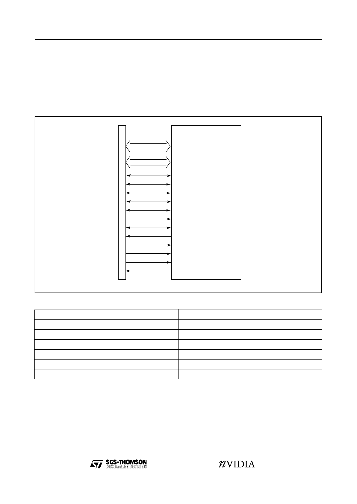
4 ACCELERATED GRAPHICS PORT (AGP) INTERFACE
The Accelerated Graphics Port (AGP) is a high performance, component level interconnect targeted at 3D
graphical display applications and based on performance enhancements to the PCI local bus.
Figure 1.
System block diagram showing relationship between AGP and PCI buses
Background to AGP
Although 3D graphics acceleration is becoming a
standard feature of multimedia PC pl atforms, 3D
rendering generally has a voracious appetite for
memory bandwidth. Consequently there is upward
pressure on the PC’s memory requirement leading
to higher bill of material costs. These trends will increase, requiring high speed access to larger
amounts of memory. The primary motivation for
AGP therefore was to contain these costs whilst
enabling performance improvements.
By providing significant bandwidth improvement
between the graphics accelerator and system
memory, some of the 3D rendering data structures
can be shifted into main memory, thus relieving
the pressure to increase the cost of the local
graphics memory.
Texture data are the first structures targeted for
shifting to system memory for four reasons:
1 Textures are generally read only, and therefore
do not have special access ordering or coherency problems.
2 Shifting textures balances the bandwidth load
between system memory and local graphics
memory, since a well cached host processor
has much lower memory bandwidth requirements than a 3D rendering engine. Texture access comprises perhaps the largest single component of rendering memory bandwi dth (compared with rendering, display and Z buffers), so
avoiding loading or caching textures in graphics
local memory saves not only this component of
local memory bandwidth, but also the bandwidth necessary to load the texture store in the
first place. Furthermore, this data must pass
through main memory anyway as it is loaded
from a mass store device.
3 Texture size is dependent upon application
quality rather than on display resolution, and
therefore subject to the greatest pressure for
growth.
4 Texture data is not persistent; it resides in
memory only for the duration of the application,
so any system memory spent on texture storage can be returned to the f ree memory heap
when the application finishes (unlike display
buffers which remain in use).
Other data structures can be moved to main memory but the biggest gai n results from moving texture data.
Relationship of AGP to PCI
AGP is a superset of the 66MHz PCI Specification
(Revision 2.1) with performance enhancements
optimized for high performance 3D graphics applications.
The PCI Specification is unmodified by AGP and
‘reserved’ PCI fields, encodings and pins, etc. are
not used.
AGP does not replace the need for the PCI bus in
the system and the two are physically, logically,
and electrically independent. As shown in Figure 1
AGP chipsetRIVA 128
System
memory
CPU
I/O I/O I/O
PCI
AGP
128-BIT 3D MULTIMEDIA ACCELERATORRIVA 128
16/77
the AGP bridge chip and RIVA 128 are the only
devices on the AGP bus - all other I/O devices remain on the PCI bus.
The add-in slot defined for AGP uses a new connector body (for electrical signaling reasons)
which is not compatible with the PCI connector;
PCI and AGP boards are not mechanically interchangeable.
AGP accesses differ from PCI in that they are
pipelined. This compares with serialized PCI
transactions, where the address, wait and data
phases need to complete before the next transaction starts. AGP transactions can only access system memory - not other PCI devices or CPU. Bus
mastering accesses can be either PCI or AGPstyle.
Full details of AGP are given in the
Accelerated
Graphics Port Interface Specification
[3] published
by Intel Corporation.
4.1 RIVA 128 AGP INTERFACE
The RIVA 128 glueless interface to AGP 1.0 is shown in Figure 2.
Figure 2.
AGP interface pin connections
4.2 AGP BUS TRANSACTIONS
AGP bus commands supported
The following AGP bus c ommands are s upported
by the RIVA 128:
- Read
- Read (hi-priority)
PCI transactions on the AGP bus
PCI transactions can be interleaved with AGP
transactions including between pipelined AGP
data transfers. A basic PCI transaction on the AGP
interface is shown in Figure 3. If the PCI target is
a non AGP compliant master, it will not see
AGPST[2:0]
and the transaction appears to be on
a PCI bus. For AGP aware bus masters,
AGPST[2:0]
indicate that permission to use the interface has been granted to initiate a request and
not to move AGP data.
AGP bus
PCICBE[3:0]#
PCIAD[31:0]
AGPPIPE#
32
4
PCIDEVSEL#
PCIIRDY#
PCITRDY#
PCISTOP#
PCIIDSEL
PCIREQ#
PCIGNT#
PCICLK
PCIRST#
PCIPAR
PCIINTA#
RIVA 128
AGPST[2:0]#
3
AGPRBF#

128-BIT 3D MULTIMEDIA ACCELERATOR RIVA 128
17/77
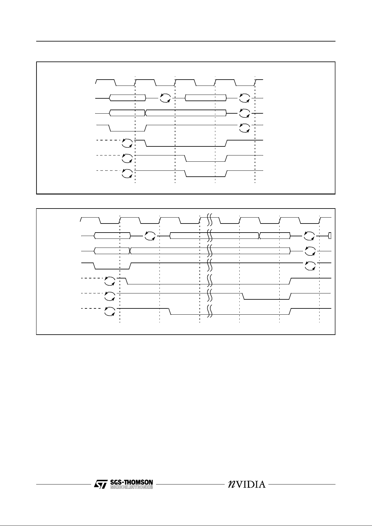
Figure 3.
Basic PCI transaction on AGP
An example of a PCI transaction occurring between an AGP command cycle and return of da ta is shown
in Figure 4. This shows the sm allest number of cycles during which an AGP request can be enqueued, a
PCI transaction performed and AGP read data returned.
Figure 4.
PCI transaction occurring between AGP request and data
bus cmd
data_pciaddress
BE[3:0]#
111 111 xxx xxx xxxxxx
PCICLK
PCIFRAME#
PCIAD[31:0]
PCICBE[3:0]#
PCIIRDY#
PCITRDY#
PCIDEVSEL#
PCIREQ#
PCIGNT#
AGPST[2:0]
134562
A9
111 xxx 111 111 xxx111
address data D7 +1
C9 pci_cmd BE 0000 000
xxx 00x xxx xxx
PCICLK
AGPPIPE#
PCIFRAME#
PCIAD[31:0]
PCICBE#
PCIIRDY#
PCITRDY#
PCIDEVSEL#
PCIAGPRBF#
PCIREQ#
PCIGNT#
AGPST[2:0]
12345678910

128-BIT 3D MULTIMEDIA ACCELERATORRIVA 128
18/77
Figure 5.
Basic AGP pipeline concept
Pipeline operation
Memory access pipelining provides the main performance enhancement of AGP over PCI. AGP
pipelined bus transactions share most of the PCI
signal set, and are interleaved with PCI transactions on the bus.
The RIVA 128 supports AGP pipelined reads with
a 4-deep queue of outstanding read requests.
Pipelined reads are primarily used by the RIVA
128 for cache filling, the cache size being optimized for AGP bursts. Depending on the AGP
bridge, a bandwidth of up to 248MByte/s is achievable for 128-byte pipelined reads. This compares
with around 100MByte/s for 128-byte 33MHz PCI
reads. Another feature of AGP is that for smal ler
sized reads the bandwidth is not significantly reduced. Whereas 16-byte reads on PCI trans fer at
around 33MByte/s, on AGP around 175MByte/s is
achievable. The RIVA 128 actually requests reads
greater than 64 bytes in multiples of 32-byte transactions.
The pipe depth can be maintained by the AGP bus
master (RIVA 128) intervening in a pipelined transfer to insert new requests between data replies.
This bus sequencing is illustrated in Figure 5.
When the bus is in an idle conditio n, the pipe can
be started by inserting one or more AGP access
requests consecutively. Once the data reply to
those accesses starts, that stream can be br oken
(or intervened) by the bus master (RIVA 128) inserting one or more additional AGP access requests or inserting a PCI transaction. This intervention is accomplished with the bus ownership
signals,
PCIREQ#
and
PCIGNT#
.
The RIVA 128 implements both high and low priority reads depending of the status of the rendering
engine. If the pipeline is likely to stall due to system memory read latency, a high priority read request is posted.
Address Transactions
The RIVA 128 requests permission from the
bridge to use
PCIAD[31:0]
to initiate either an
AGP request or a PCI transaction by asserting
PCIREQ#
. The arbiter grants permission by as-
serting
PCIGNT#
with
AGPST[2:0]
equal to ‘111’
(referred to as START). When the RIVA 128 receives START it must start the bus operation within two clocks of the bus becoming available. F or
example, when the bus is in an idle condition when
START is received, the RIVA 128 must initiate the
bus transaction on the next clock and the one following.
Figure 6 shows a single address being enqueued
by the RIVA 128. Sometime before clock 1, the
RIVA 128 asserts
PCIREQ#
to gain permission to
use
PCIAD[31:0]
. The arbiter grants permission
by indicating START on clock 2. A new request
(address, command and length) are enqueued on
each clock in which
AGPPIPE#
is asserted. The
address of the request to be enqueued is presented on
PCIAD[31:3]
, the length on
PCIAD[2:0]
and
the command on
PCICBE [3:0] #
. In Figure 6 only
a single address is enqueued since
AGPPIPE#
is
just asserted for a single clock. The RIVA 128 indicates that the current address is the last it intends to enqueue when
AGPPIPE#
is asserted
and
PCIREQ#
is deasserted (occurring on clock
3). Once the arbiter detects the assertion of
AGP-
PIPE#
or
PCIFRAME#
it deasserts
PCIGNT#
on
clock 4.
Bus Idle
Pipelined
data
transfer
Intervene
cycles
Pipelined AGP re quests
A1 A2
Data-1 Data-2
A3
PCI transaction
A
Data
Data-3
128-BIT 3D MULTIMEDIA ACCELERATOR RIVA 128
19/77
Figure 6.
Single address - no delay by master
Figure 7 shows the RIVA 128 enqueui ng 4 requests, whe re the first r equest is delayed by the maximum
2 cycles allowed. START is indicated on clock 2, but the RIVA 128 does not assert
AGPPIPE#
until clock
4. Note that
PCIREQ#
remains asserted on clock 6 to indicate that the current request is not the last one.
When
PCIREQ#
is deasserted on clock 7 with
AGPPIPE#
still asserted this indicates that the current ad-
dress is the last one to be enqueued during this transaction.
AGPPIPE#
must be deasserted on the next
clock when
PCIREQ#
is sampled as deasserted. If the RIVA 128 wants to enqueue more requests during
this bus operation, it continues asserting
AGPPIPE#
until all of its requests are enqueued or until it has
filled all the available request slots provided by the target.
Figure 7.
Multiple addresses enqueued, maximum delay by RIVA 128
C1
A1
111 111 xxx xxx xxxxxx xxx xxx
PCICLK
AGPPIPE#
PCIAD[31:0]
PCICBE[3:0]#
PCIREQ#
PCIGNT#
AGPST[2:0]
12345678
A1
111 111 111 xxx xxxxxx xxx xxx
A2 A3 A4
C1 C2 C3 C4
PCICLK
AGPPIPE#
PCIAD[31:0]
PCICBE#
PCIREQ#
PCIGNT#
AGPST[2:0]
1234567
128-BIT 3D MULTIMEDIA ACCELERATORRIVA 128
20/77
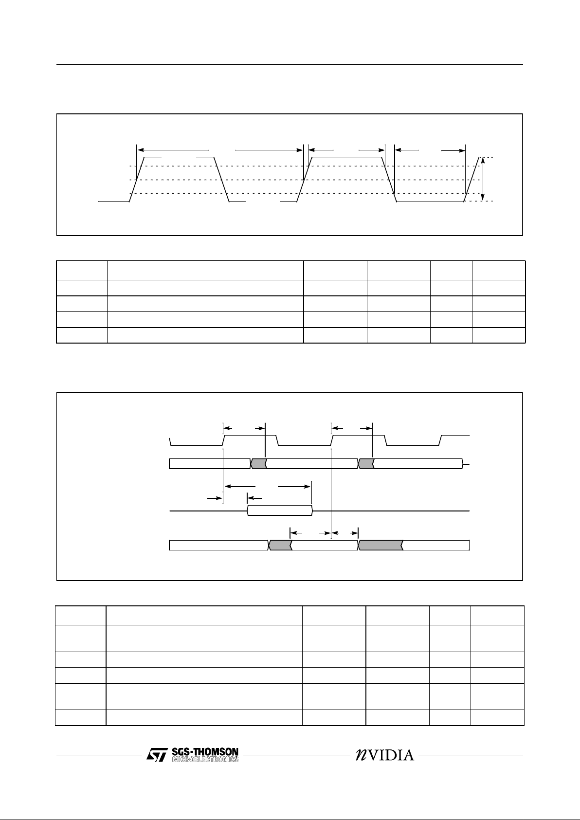
AGP timing specification
Figure 8.
AGP clock specification
Table 1.
AGP clock timing parameters
NOTES
1 This rise and fall time is measured across the minimum peak- to- peak ra nge as shown in Figure 8.
Figure 9.
AGP timing diagram
Table 2.
AGP timing parameters
Symbol Parameter Min. Max. Unit Notes
t
CYC
PCICLK
peri od 15 30 ns
t
HIGH
PCICLK
high ti me 6 ns
t
LOW
PCICLK
low time 6 ns
PCICLK
slew rate 1.5 4 V/ns 1
Symbol Parameter Min. Max. Unit Notes
t
VAL
AGPCLK
to signal valid delay (da ta and control
signals)
211ns
t
ON
Float to active delay 2 ns
t
OFF
Active to float delay 28 ns
t
SU
Input set u p time to
AGPCLK
(data and contro l
signals)
7ns
t
H
Input hold time from
AGPCLK
0ns
t
CYC
t
HIGH
t
LOW
PCICLK
0.3VDD
0.4VDD
0.5VDD
0.2VDD
0.6VDD
2V p-to-p
(minimum)
t
VAL
t
VAL
t
ON
t
OFF
t
SU
t
H
data1 data2
data1 data2
AGPCLK
Output delay
Tri-state outpu t
Input
128-BIT 3D MULTIMEDIA ACCELERATOR RIVA 128
21/77
5 PCI 2.1 LOCAL BUS INTERFACE
5.1 RIVA 128 PCI INTERFACE
The RIVA 128 supports a glueless interface to PCI 2.1 with both master and slave capabilities. The host
interface is fully compliant with the 32-bit PCI 2.1 specification.
The Multimedia Accelerator supports PC I bus operation up to 33MHz with z ero-wait s tate capability and
full bus mastering capability handling burst reads and burst writes.
Figure 10.
PCI interface pin connections
Table 3.
PCI bus commands supported by the RIVA 128
Bus master Bus slave
Memory read and write Memory read and write
Memory read line I/O read and wr it e
Memory read multiple Configuration read and write
Memory read line
Memory read multiple
Memory write invalidate
PCI bus
PCICBE[3:0]#
PCIAD[31:0]
PCIFRAME#
32
4
PCIDEVSEL#
PCIIRDY#
PCITRDY#
PCISTOP#
PCIIDSEL
PCIREQ#
PCIGNT#
PCICLK
PCIRST#
PCIPAR
PCIINTA#
RIVA 128
128-BIT 3D MULTIMEDIA ACCELERATORRIVA 128
22/77
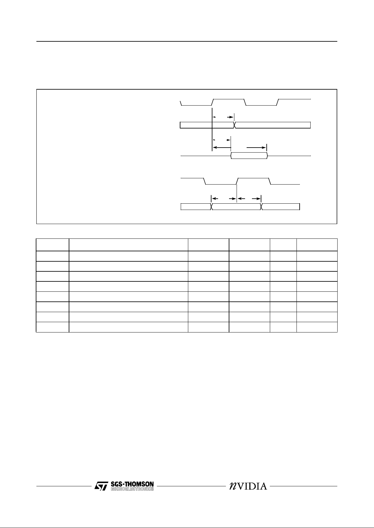
5.2 PCI TIMING SPECIFICATION
The timing specification of the PCI interface takes the form of generic setup, hold and delay times of tran-
sitions to and from the rising edge of
PCICLK
as shown in Figure 11.
Figure 11.
PCI timing parameters
Table 4.
PCI timing parameters
NOTE
1
PCIREQ#
and
PCIGNT#
are point to point signals and have different valid delay and input setup times tha n bussed sig-
nals. All other signals are bussed.
Symbol Parameter Min. Max. Unit Notes
t
VAL
PCICLK
to signal valid delay (buss ed sig nals) 2 11 ns 1
t
VAL
(PTP)
PCICLK
to signal valid delay ( poi nt to point) 2 12 ns 1
t
ON
Float to active delay 2 ns
t
OFF
Active to float delay 28 ns
t
SU
Input set u p time to
PCICLK
(bussed signals) 7 ns 1
t
SU
(PTP)
Input set u p time to
PCICLK (PCIGNT#
)10 ns1
t
SU
(PTP)
Input set u p time to
PCICLK (PCIREQ#
)12 ns
t
H
Input hold time from
PCICLK
0ns
t
VAL
t
ON
t
OFF
t
SU
t
H
PCICLK
Output delay
Tri-state output
Input
PCICLK
Output timing parameters
Input timing parameters
128-BIT 3D MULTIMEDIA ACCELERATOR RIVA 128
23/77
Figure 12.
PCI Target write -
Slave Writ
e (single 32-bit with 1-cycle
DEVSEL#
response)
Figure 13.
PCI Target write - Slave Write (multiple 32-bit with zero wait state
DEVSEL#
response)
address data
bus cmd BE[3:0]#
(med)
PCICLK
PCIAD[31:0]
PCICBE[3:0]#
PCIFRAME#
PCIIRDY#
PCITRDY#
PCIDEVSEL#
address data0
bus cm d BE[3: 0]#
data1 data2
BE[3:0]# BE[3:0]#
PCICLK
PCIAD[ 31:0]
PCICBE[3:0]#
PCIFRAME #
PCIIRDY#
PCITRDY#
PCIDEVSEL#
128-BIT 3D MULTIMEDIA ACCELERATORRIVA 128
24/77
Figure 14.
PCI Target read - Slave Read (1-cycle s ingle word read)
Figure 15.
PCI Target read - Slave Read (slow single word read)
address
bus cmd BE[3:0]#
data0
PCICLK
PCIAD[31:0]
PCICBE[3:0]#
PCIFRAME#
PCIIRDY#
PCITRDY#
PCIDEVSEL#
address
bus cmd BE[3:0]#
data0
PCICLK
PCIAD[31:0]
PCICBE[3:0]#
PCIFRAME#
PCIIRDY#
PCITRDY#
PCIDEVSEL#
 Loading...