

SGS Thomson Microelectronics STFLWARP20-PL Datasheet
March 1996
This isadvance informationon a new product now in development or undergoing evaluation. Details are subject to changewithoutnotice.
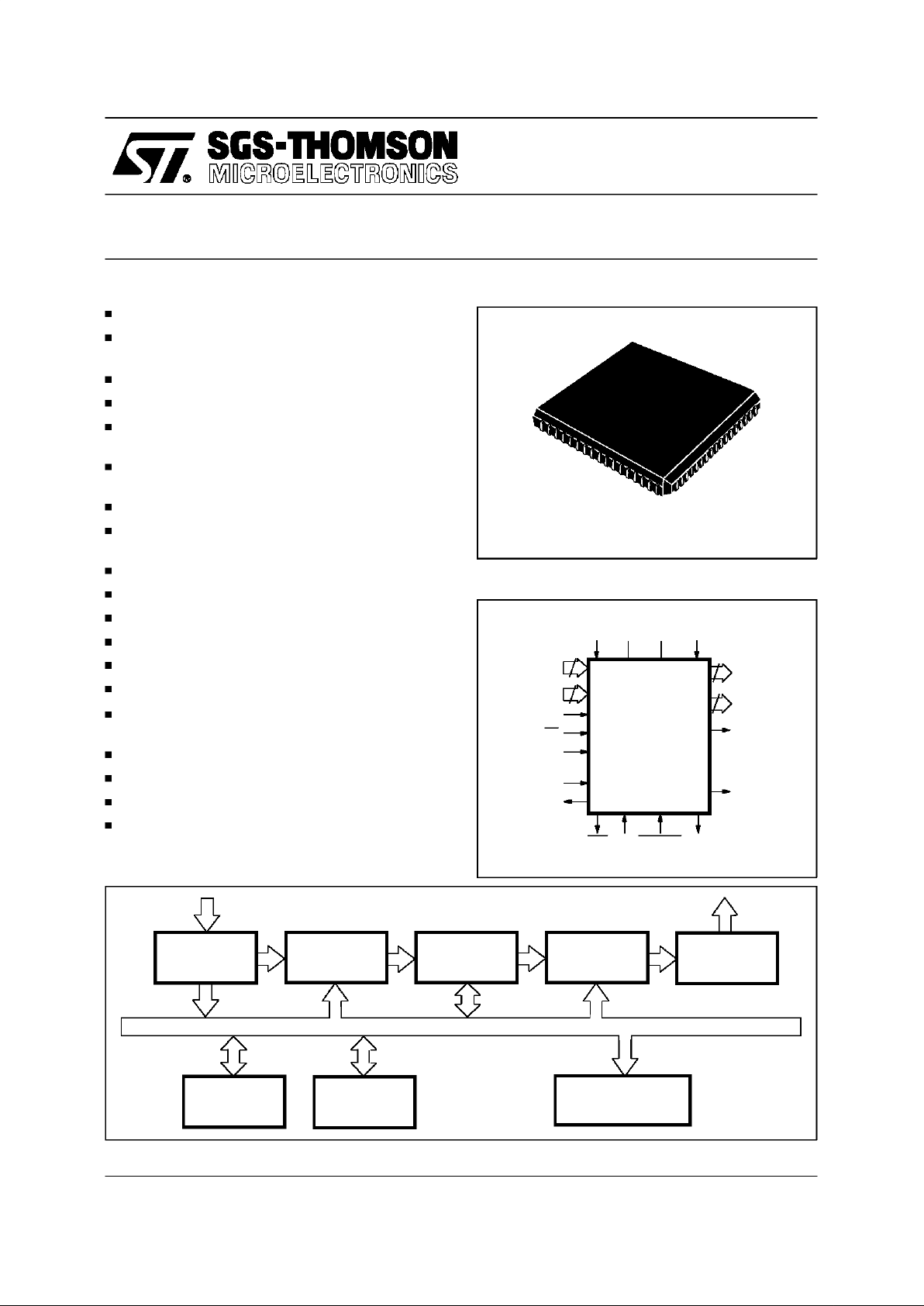
PLCC68
8
I0-I7
BUSYOFL
12
O0-O11
2
OC0-OC1
DS
PRESET
VSS VDD
W.A.R. P .
2.0
LASTIN
MCLK WAIT
ENDOFL
ERR
OE
AUTO
3
SIS0-SIS2
RD
READY
Figure1. Logic Diagram.
Digital Fuzzy Co-processor8-bit I/O
HighSpeed Rules Processing
4 Input, 2 Output,32 Rules in 33.1µs
Upto 256Rules(4 Antecedents,1 Consequent)
Up to 8 Input ConfigurableVariables
Up to 16 MembershipFunctions for an Input
Variable
AntecedentMembershipFunctions with
Triangular and TrapezoidalShape
Up to 4 Output Variables
Up to 256 MembershipFunctionsfor all
Consequents
SingletonConsequentMembership Functions
Defuzzification on chip
MaximumClock Frequency40MHz
A/D Start Convertion Pulse presettable
Direct Interfaceto all popular microprocessor
HandshakingSignal Polarity presettable
Operates”STANDALONE” (without µP) if
desired
Standard+5V Supply Voltage
SoftwareTools and EmulatorsAvailability
Pinnumber: 52
68-leadPlastic Leaded Chip Carrierpackage.
ANTECEDENT
MEMORY
PROGRAM &
CONSEQUENT
MEMORY
PROGRAMMABLEA/D
OUTPUT PULSE
INTERNALBUS
Input Port
with
HANDSHAKE
8
ALPHA
CALCULATOR
INFERENCE
UNIT
DEFUZZIFIER
Ouput Port
with
HANDSHAKE
8
Figure2. SimplifiedBlock Diagram.
W.A.R.P.2.0
8-BIT FUZZY CO-PROCESSOR
PRELIMINARYDATA
1/28
GENERAL DESCRIPTION
W.A.R.P.2.0is a memberof the W.A.R.P. family of
fuzzy microprocessors, completelydevelopedand
producedbySGS-THOMSONMicroelectronicsusing the high performance, reliable HCMOS4T
(O.7µm)process.
W.A.R.P.2.0can beused bothas a Fuzzy Co-proc-
essor or as a stand-alone microcontroller. In the
former case, it can work together with standard
micros which shall perform normal control tasks
whileW.A.R.P.2.0 willbeindipendentlyresponsible
for all the fuzzy related computing.
W.A.R.P.2.0 core includes the fuzzifier (ALPHA
calculator),the inference unit, and the defuzzifier.
The I/O capabilities demandedby microprocessor
applicationsarefulfilledbyW.A.R.P.2.0with 8Input
and 4 Output lines which can be supported by
handshakingsignals.
The capability of preset the polarity of the handshaking signals simplifies the interface with the
host processor.
An internal Start Conversion pulse is provided to
allow simple use for waveform generation which
canbe directly applied to drivean A/D converter.
The output 3-STATE buffer can be temporarily
frozen in order to synchronize W.A.R.P.2.0 with
slower devices.
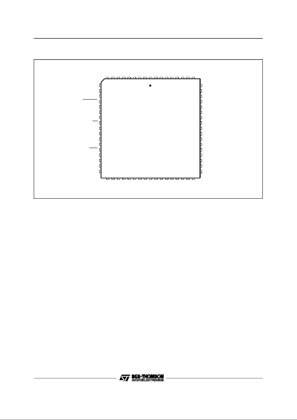
9 8 7 6 5 4 3 2 1 68 67 66 65 64 63 62 61
2728 29 30 31 32 33 34 35 36 37 3839 40 41 42 43
16 15 14 13 12 1110
44 45 46 47 48 49 50 51 52 53 54 55 56 57 58 59 60
W.A.R.P. 2.0
nc
nc
nc
VDD
VSS
O0
O1
O2
O3
O4
O5
O6
VDD
VSS
nc
nc
nc
VSS
VDD
MCLK
PRESET
OFL
AUTO
LASTIN
OE
RD
TEST
DS
ENDOFL
ERR
BUSY
READY
VSS
VDD
ncncI7I6I5I4I3I2VSSI1I0
WAIT
SIS0
SIS1
SIS2ncnc
ncncnc
VSS
VDD
OC1
OC0
O11
O10
O9O8O7
VSS
VDD
ncncnc
26 25 24 23 22 21 20 19 18 17
Figure3. Pin Connections
Running W.A.R.P.2.0 involves a downloading
phase and an On-Line phase. The downloading
phase allows thesetting of the processor,in terms
of I/O number,universeof discourse,Membership
Functions (MFs) and rules. During this phase
W.A.R.P.2.0 preparesits internal memoriesfor the
On-Line elaboration phase and loads the microcodeinitsprogrammemory.Thismicrocode,which
drives the On-Line phase, is generated by the
Compiler (see FUZZYSTUDIO2.0 User Manual).AfterthatW.A.R.P.2.0isreadytorun (On-Line
phase) processing inputs and producing the related outputsaccordingto theconfigurationloaded
in the downloading phase. It is also possible to
provide the processor with inputs in any order by
specifyingtheir identificationnumbers.
Two basic memories are available in W.A.R.P.2.0 :
the Anteced ent Memory (AM) and the Program/Consequent Memory (PCM). The antecedentMFs,portrayedbyaresolutionof 2
8
elements,
are stored in the AM (256 bytes). W.A.R.P.2.0
exploits a SGS-THOMSON patented strategy to
store the MFs in the AM.
The informationaboutRules andConsequentMFs
are stored in the PCM (1.4 Kbyte).
FUZZYSTUDIO2.0 is a powerful development
environment consisting of board and software allowsan easyconfigurationanduse ofW.A.R.P.2.0.
Note:nc = Not Connected.
2/28
W.A.R.P.2.0

Pin Assignment Name Pins Type Function
11,26,31,40,48,57 VDD - Power Supply
1,10,25,30,39,47,56 VSS - Ground
19 TEST I Testing(It must be connected to VSS)
12 MCLK I Master Clock (up to 40 MHz)
13 PRESET I Preset
15 AUTO I Auto/Manual-Boot
65 SIS0 I
Auto-Boot Speed (Ext. Memory Support AccessTime) /
Input Selection bit 0
64 SIS1 I
Auto-Boot Speed (Ext. Memory Support Access Time) /
Input Selection bit 1
63 SIS2 I
Auto-Boot Speed (Ext. Memory Support Access Time) /
Input Selection bit 2
67 I0 I Data Input bit 0
68 I1 I Data Input bit 1
2 I2 I Data Input bit 2
3 I3 I Data Input bit 3
4 I4 I Data Input bit 4
5 I5 I Data Input bit 5
6 I6 I Data Input bit 6
7 I7 I Data Input bit 7
14 OFL I Off-Line/On-Line Switch
18 RD I Handshaking Read Ready
16 LASTIN I Last Input (Start Elaboration) bit
17 OE I Output Enable/3-STATEbit
66 WAIT I Temporary Output Processing Stop
24 READY O Handshaking Output Signal
21 ENDOFL O Offline Phase (external memory downloading) End
23 BUSY O Elaboration Phase Indicator
20 DS O Data Strobe (Output Ready Signal)
22 ERR O ErrorFlag
33 OC0 O Output Identifier bit 0
32 OC1 O Output Identifier bit 1
55 O0 O External Memory Address/Defuzzified Output bit 0
54 O1 O External Memory Address/Defuzzified Output bit 1
53 O2 O External Memory Address/Defuzzified Output bit 2
52 O3 O External Memory Address/Defuzzified Output bit 3
51 O4 O External Memory Address/Defuzzified Output bit 4
50 O5 O External Memory Address/Defuzzified Output bit 5
49 O6 O External Memory Address/Defuzzified Output bit 6
38 O7 O External Memory Address/Defuzzified Output bit 7
37 O8 O
ExternalMemory Address bit 8 /
Next Input Progressive Number bit 0
36 O9 O
ExternalMemory Address bit 9 /
Next Input Progressive Number bit 1
35 O10 O
External Memory Address bit 10 /
Next Input Progressive Number bit 2
34 O11 O
External Memory Address bit 11 /
Start Conversion for the externalA/D
Table 1. Pin Description
3/28
W.A.R.P.2.0

PINDESCRIPTION
Signals READY, RD, WAIT, DS, BUSY, LASTIN
and O11 ( external A/D Start Conversion) have
programmable polarity, see table 6 for default
values.
V
DD
,VSS. Power is supplied to W.A.R.P. using
these pins.V
DD
isthe powerconnectionand VSSis
the ground connection;multi-connectionsare necessary.
MCLK.
Master Clock
(Input): This is the input
master clock whose frequency can reach up to
40MHz(MAX).
During the Off-Line phase with AUTO High, the
MCLKis internallydividedto utilize boot memories
workingwitha slowerfrequency.Theaccessspeed
is presettableby means of SIS0-SIS2pins.
PRESET.
Preset
(Input, active Low) : This is the
restart pin of W.A.R.P.. It is possible to restart the
work during the computation (On-Line phase) or
before the writing of internal memories (Off-Line
phase). In both cases it must be put Low at least
for a clock period. After PRESET Low the processor remainsin the resetstatus 3 MCLK pulses.
AUTO.
Auto-Boot:
(Input,activeHigh): During the
Off-Linephase AUTOHigh enables the automatic
bootof W.A.R.P.2.0 whereas AUTO Lowvalidates
the manual downloading.The manualboot has to
be performed using the handshaking signals
RD/READY.
During the On-Line phase AUTO High disables
the generation of the Start A/D conversion (O11)
signal.
SIS0-SIS2.
Speed& Input Selection
(Inputs): DuringtheOff-Linephase withAUTOHigh(Auto-Boot)
SISbus allowstochoosethespeedofdownloading
fromthe externalmemorywhich containsthestartupconfigurationof W.A.R.P.2.0.In thatcase (AutoBoot)MCLKisinternallydividedtoprovideaslower
sinchronizationsignal which is automaticallyused
asRDfor thereadingof theexternalmemory.Table
2 shows how to preset the frequency of thissynchronizationsignal.
During the On-Line phase in Slave mode (see
RegisterBench description,Tab.5)SIS bus allows
to provide W.A.R.P.2.0with inputs in any order by
specifying their identification number. The input
and its identification number (SIS0-SIS2) will be
acquired at the next active RD so they must be
already stable when RD is given.
SIS0 SIS1 SIS2
Internal Synchronization
Signal Frequency
Low Low Low MCLK/32
High Low Low MCLK/16
Table2. DownloadingSpeed
I0-I7.
Input bus
(Input): During the Off-Linephase
these 8 data inputpins acceptaddresses anddata
from the e xte rna l boot memory cont aining
W.A.R.P.2.0 configuration. This start-up memory
(which can be a ZERO-POWER,the host processor memory, an EPROM, a Flash,the PC Memory,
etc.) contains the fuzzy project built by means of
FUZZYSTUDIO2.0.
In On-Linemodethisbuscarriestheinputvariables
accordingto the prefixedorder.
OFL.
Offline
(Input, active High): When this pin is
High,the chipisenabledtoloaddataintheinternal
RAMs (Off-Linephase). It must be Low when the
fuzzy controller is waiting for input values and
during the processingphase (On-Linephase).
When OFL changes its status the processor remains presettedfor 3 clockpulses.
LASTIN.
Last Input
(Input, default active High):
During the On-Line phase in slave mode (see
RegisterBench description,table 5) LASTINHigh
indicates no other inputs have to be provided so
W.A.R.P.2.0 canstart the processing phase.
W.A.R.P.2.0 inputs are those in the input interface
so if some variables do not need to be acquired
again (because they change slower than others)
they remainstored and no extra time isrequired to
acquire them again.
OE.
Output Enable
(Input, active Low): OE Low
enables O0-011output bus or (if High) put it in
3-STATE.
WAIT.
Wait
(Input, default active High): This pin
High stops the output processing. When WAIT is
enabled W.A.R.P.2.0 finishes to compute the current output variable but it does not give it on the
output bus until WAIT becomes Low. This signal
allows to synchronize W.A.R.P.2.0with slower devices.
RD.
Read
(Input, default active High): Both in
Off-Line and in On-Line mode RD indicates data
are ready tobe acquired from the input bus I0-I7.
READY.
Ready
(Output,default active High): Both
in Off-Lineand in On-Linemode RDindicates data
have been acquired from the input bus I0-I7 and
are now stored in W.A.R.P.2.0 internal registers.
ENDOFL.
End of Off-Line phase
(Output, active
High): This pin indicates the end of the downloading phase (Off-Line) so the content of the boot
memory is already stored in W.A.R.P.2.0 internal
memories.After ENDOFLis activetheusercan put
OFL Low so the On-Linephase canstart.
BUSY.
BusySignal
(Output, defaultactive High):
When the elaborationphase is running this pin is
active. When W.A.R.P.2.0finishesto compute the
last output variable, it puts BUSY Low and waits
for new inputs.
4/28
W.A.R.P.2.0

DS.
DataStrobe
(Output, defaultactive High): The
strobe pin enables the user to utilize the output.
Whenthispin is High itindicatesthat a new output
variablehas beencalculatedand it is ready on the
output bus (O0-O7). This signal synchronizes the
external devices and in particular the interfaces
with the controlledprocesses (On-Line mode).
ERR.
Error
(Output, activeLow): When this pin is
active,W.A.R.P.2.0has incurredin an internalerror
condition.
OC0-OC1.
Output Counter
(Output): This 2 bit
output bus provides the output variables with a
progressivenumber during the On-Line phase.As
a consequence it is possible to know to which
variablecorrespond thedata thatare onthe output
data bus (O0-O7). The dimension of OC bus is
connected with the maximum number of output
variables(4).
O0-O11.
Output Bus
(Output): In the Off-Line
phasethese pins providethe addresses (12bit) for
its internalmemories and send those addresses to
theexternalmemorysupportwheredatatoloadare
located. These addresses sent on O0-O11 bus
allow to identify the data that have to be loaded in
W.A.R.P.2.0internal memories.
In the On-Line phase O0-O7 carrie out the output
values. When the DS is High, one output variable
can be read by external devices. The resolution
of output variables is 256 points (8 bit). If there is
more than one output, the output variables are
calculated one by one and they are provided in
the sequence stabilized during the editing phase
(see FUZZYSTUDIO 2.0 User Manual).
In On-Line mode O8-O10 provide the progressive
numberof the next variable to be acquired. These
pinscan beused to select the next input to provide
on I0-I7 bus.
Stillinon-line modeO11allows toprovideapresettablesignal whichcan beusedasStart-Conversion
for an A/D converter after (about 400 ns) OFL or
BUSY fall.
5/28
W.A.R.P.2.0

FUNCTIONAL DESCRIPTION
W.A.R.P.2.0 works in two modedependingon the
OFL controlsignal level (see table 3) :
Off-line MODE (OFL High)
On-line MODE(OFL Low)
OFF-LINE MODE
All W.A.R.P. memories are loadedduring the OffLine phase. The membershipfunctions are written
insidetheir relatedmemories andthe processcontrol rules are loaded inside the PCM.
The addresses of the words to be written in the
memories, are internally generated while the addresses of the external memory locations to be
readaredirectlyprovidedbyW.A.R.P.2.0bymeans
of O0-O11output pins.
Data must be loaded 8 bit a time in the data bus
and can be read from an external non volatile
memoryor loaded by an host processor.
The Off-Line phase can be performed automatically (see figure4) or manually(see figure 5).
When the auto-boot is chosen (AUTO = High)it is
possibleto configurethereadingaccesstimeof the
externalmemory. Theauto-bootendis indicatedby
the ENDOFLsignal.
The downloadingphase requires:
F*NWordsDatabaseclock pulses,
where F is 16 or 32 (see table 2).
NWordsDatabaseis the number of wordsstoredin
the boot-memory (see register bench description,
table 5).
When the manual-boot is chosen (AUTO = Low)
datahave to beprovidedby usingthe handshaking
signals (RD/READY). In this way it is possible to
updateonly aportionofthe databaseorchangethe
processorconfiguration.
The time required from the manual boot depends
on the efficiency of the communication handled
with the handshakingsignals.
W.A.R.P.2.0
BOOT
MEMORY
OFLAUTO
HH
ENDOFL
I0-I7
O0-O11
SIS0-SIS2
Auto-Boot Enable
AUTO=HIGH
Off-linePhase Enable
OFL=HIGH
OFFLINEPHASE ENDS
ENDOFL=HIGH
External Memory
Access Time SETTING
SIS0-SIS2=LowLow...
DownloadingFrom
External Memory
Figure 4. Off-Linephase:Auto-Boot
Manual-Boot Enable
AUTO=LOW
Off-linePhase Enable
OFL=HIGH
OFFLINE PHASE ENDS
Downloading with
Handshaking Signals
RD/READY
W.A.R.P.2.0
BOOT
MEMORY
OFLAUTO
LH
READY
I0-I7
O0-O11
RD
Figure 5. Off-LinePhase: Slave Downloading
6/28
W.A.R.P.2.0
ON-LINEMODE
In On-line mode (see figure 7) W.A.R.P.2.0 is enabled to elaborate input values and calculate outputs according to the fuzzy rules stored into the
microprogram. W.A.R.P.2.0 reads the inputvalues
one a time in the input data bus using the
RD/READY signals. If the processor is workingin
SLAVE mode (see register bench description in
table5) the user has toprovidethe inputswith their
identificationnumbers(bymeansofSIS0-SIS2),so
it is possible to provide inputs in any order. In
SLAVE mode it is also po ssible to force
W.A.R.P.2.0 to start the elaboration phase (by
means of LASTIN) without providing all inputs, for
instancewhen inputvariableschangewithdifferent
speed. In this case the outputs that have not be
providedin this cycle,but sampled in the previous
ones, are recoveredfrom the internalbuffers.
When all inputs are given or a LASTIN signal is
given, the elaboration phase starts. The elaboration phase is divided in two main parts. During the
first one the input values are read and the correspondingALPHAvalues(activationlevels)are calculated.In thesecond part the computation of the
fuzzy rules and the defuzzification are implemented.
W.A.R.P.2.0 acquires each input in 8 clock pulses
(min). Sincethe acquisition phase is performedby
the user by means of the handshaking signals, 8
clock pulses per input are referred to the most
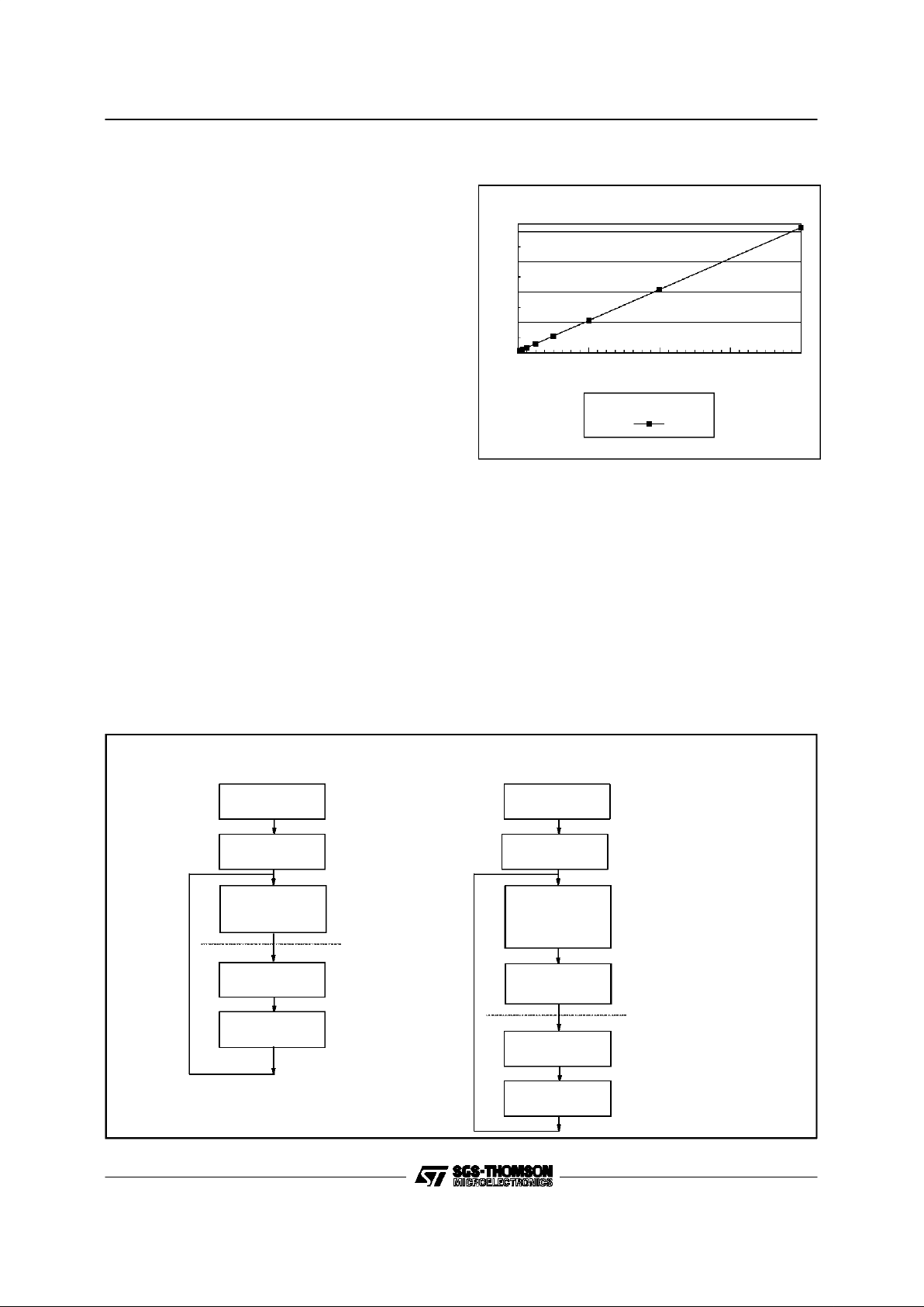
efficient case. In figure 6 are shown the perform-
0 64 128 192 256
0
2.000
4.000
6.000
8.000
Numbe r of Rule s
Numbe r of Clock Pu ls e s
Numb er of I np u t s = 8
Figure6. W.A.R.P.2.0 performances
ances in case of 8 inputs. If you are using less
inputs you have to subtract 8 clock pulsesfor each
of them. The elaboration time for rule requires 32
clockpulses.
For instance if W.A.R.P.2.0 is working at a frequency of 40 MHz (25ns period)with 8 inputs and
128 rules globally(forall outputs) thetime required
to provide all outputs is 4000clkp*25ns= 100µs.
On-line Phase Master
(”MASTER”se t in the register ben ch)
On-line Phase Enable
OFL=LOW
Inputs Acquisition with
Handshaking Signals
(RD/READY)
CHIP PRESET
End of Acquisition Phase
Start Elaboration Pha se
Elaboration P ha se
Outputs Gen eration
DS=HIGH
On-line Pha se Slave
(”SLAVE” set in the register bench)
On-line Phase Enable
OFL=LOW
Acquisition with
Hands haking by
specifying which inputs
is on the input bus by
means of SIS0-SIS2
CHIP PRESET
End of Acquisition Phase
Start Elaboration Pha se
Elaboration P hase
Outputs Ge neration
DS=HIGH
Last Input has been
given
LASTIN=HIGH
Figure7. On-Linephase
7/28
W.A.R.P.2.0

Mode PRESET OFL AUTO OE I0-I7 RD SIS0-SIS2 O0-O7 O8-O10 O11 OC0-OC1
Off-Line
Slave
V
IH
V
IH
V
IL
X Data In X X X X X
Off-Line
Autoboot
V
IH
V
IH
V
IH
V
IH
Data In X
Clock
Rate
Selection
Code
External Memory
Addresses
X
On-Line
Master
(2)
V
IH
V
IL
X
(2)
V
IH
Data In X
Data
Out
Next
Input
(2)
Output
Selection
On-Line
Slave
(3)
V
IH
V
IL
X
(2)
V
IH
Data In
Input
Selection
Data
Out
X
(2)
Output
Selection
Output
Disable
V
IH
XXVILX X X Hi-Z X
Reset
(4)
XXXX X XVOLV
OL
V
OL
V
OL
Table 3. OperatingModes (1)
Notes: 1. This table uses default active handshaking signal polarity (see table 6), X = don’t care.
2. If AUTO is High pulse in O11 is absent.
3. LASTIN and WAIT pulses are optional.
4. Same operation is obtained whenpositive and negative OFL transactions occour.
INTERNAL STRUCTURE
The blockdiagram shown in figure 2 describesthe
structure of W.A.R.P.2.0 (a more detailed block
diagramis shown in fig. 11).
Input Port. This internal block performs the input
datarouting.Dataareread onebytea timefrom the
input data bus, internally stored, and sent to the
ALPHA calculator following the rules loaded in the
ProgramMemory. Input data resolution is 8 bit.
The cycle starts when all inputs or a LASTIN High
have been provided and continues until BUSY is
active or a PRESET signal is given. When BUSY
becomesinactiveanewacquisitionphasecanstart.
Alpha Calculator. This block calculates the intersection (ALPHA weight) between an Antecedent
MembershipFunction and the correspondingcrisp
input (see figure 8).
InferenceUnit. Thanksto the Theta Operator,the
InferenceUnitgenerates theTHETA weightswhich
are used to manipulate the consequentMFs.
This is a calculation of the maximum and/or minimumperformed onALPHA values accordingto the
logical connectivesof fuzzy rules. It is possible to
utilize the AND/OR connectivesand to directly exploit ALPHA weights or the negated values. The
numberof THETA weights depends onthe number
of rules.
The rules can have at maximum four ALPHA
weights(howevertheyareconnected).Twoormore
rules can be only joined with the OR connective.
InferenceUnit structure is shown in figure9.
Defuzzifier. It generates the output crisp values
implementingthe consequentpart of the rules.
In thismethod consequentMFs are multiplied by a
weight value Ω (OMEGA), which is calculated on
the basis of antecedentMFsand logicaloperators.
The processing of fuzzy rules produces, for each
output variable, a resulting membership function.
Each MF related to the processed output variable
is firstly modifiedby arule weight.
Outputvalue (Y)isdeduced fromthe centroids(X
i
)
and the modified MFs (Ω
i
) byusing the formula:
Y
=
∑
1
n
Ωi∗
X
i
∑
1
n
Ω
i
n = number of MFs of the Output Variable.
X
i
=absciss ofthe MFicentroid.
Ω
i
=membership degree of the output MFi.
Two parallel blocks calculate the numerator and
denominator values to implement the centroids
formula.A finaldivision blockcalculatestheoutput
values (see figure10).
8/28
W.A.R.P.2.0

Output Port. This block provides the output data
supported by handshaking signals. Ouput data
resolutionis 8 bit.
An output ready on the bus O0-O7 is indicated by
a DS pulse and by its identificationnumber (OC0OC1). WAIT active temporarily stops the elaborationphaseallowingthesynchronizationwithslower
devices.
Programmable A/D output pulse. This block allowsto programthe widthof the pulse providedon
O11(only in On-Line mode)that can beused as a
StartConversion foran externalA/D. Thewidth of
this pulse can be configured by means of the
related register (see register bench description)
followingthe table 4.
Start conversion
Pulse Register
Pulse Width
(T
CLK
= MCLK Period)
Low,Low, Low 128xT
CLK
Low,Low, High 256xT
CLK
Low,High, Low 2040xT
CLK
Low,High, High 4080xT
CLK
High, Low, Low 8160xT
CLK
High, Low, High 16320xT
CLK
High, High, Low 32000xT
CLK
High, High, High 65520xT
CLK
Table 4. Start ConversionPulse (O11) Width
Setting.
9/28
W.A.R.P.2.0
 Loading...