

SGS Thomson Microelectronics STFLWARP11-PG Datasheet
W.A.R.P. 1.1
WEIGHT ASSOCIATIVE RULE PROCESSOR
ADVANCED DATA
HighSpeed Rules Processing
AntecedentMembership Functions with any
Shape
Up to 256Rules (4Antecedents,1
Consequent)
Up to 16 Input ConfigurableVariables
Up to 16 MembershipFunctionsforan Input
Variable
Up to 16 OutputVariables
Up to 128 MembershipFunctionsforall
Consequents
MAX-DOT Inference Method
Defuzzification on chip
SoftwareTools and EmulatorsAvailability
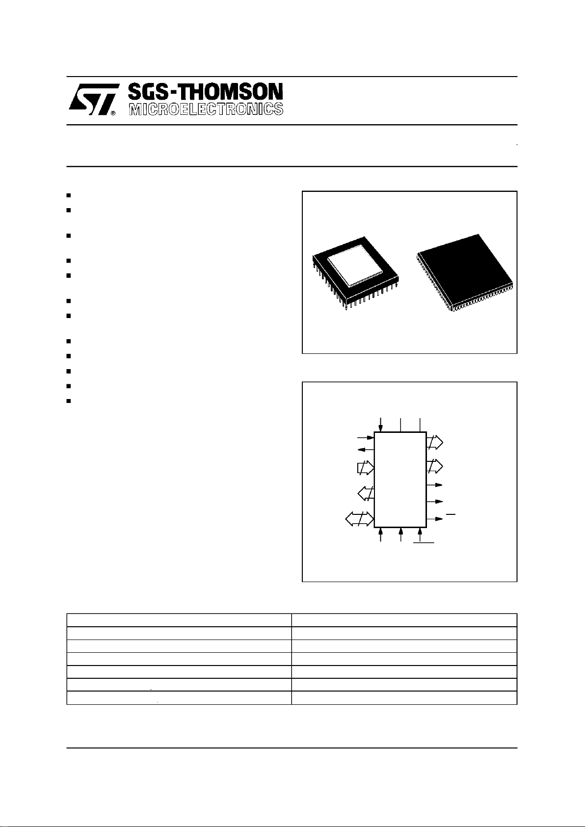
100-pinCPGA100Ceramic Package
84-leadPlastic LeadedChip Carrierpackage
GENERAL DESCRIPTION
W.A.R.P. is a VLSI Fuzzy Logic controller whose
architecture arises from the need of realizing an
integratedstructurewith high inferencingperformancesandflexibility. Toget those resultsa modular
architecture based on a set of parallel memory
blockshas beenimplemented.
Inordertoobtainhigh performancesW.A.R.P.uses
different data representations during the various
phases of the computational cycle, so that it is
always operating on the o ptimal data representation. A vectorial characterization has been
adopted for the Antecedent Membership Functions. W.A.R.P. exploits a SGS-THOMSON patentedstrategytostoretheAntecedentMembership
May 1996
This is advance information on a new productnow in development or undergoing evaluation. Details are subject to change without notice.
8
I0-I7
A0-A9
10
O0-O9
FIN
3
CHM OFL
4
OCNT0-OCNT3
STB
EP
NP
PRST
MCLK VS S VDD
W.A.R.P.
1.1
10
EPA0-EPA2
SYNC
Figure1. Logic Diagram
Number of Inputs Configurable [1..8]
Standard Rule Format 4 Antecedents, 1 Consequent [or subsets]
Rules Number Max 256 Rulesin the 4Antecedent, 1 Consequent format
Antecedent’sMFs Number Configurable [up to 16 for an input variable]
Consequent’sMFs Number Max 256 for all outputs variables
Input Data Resolution 8 bit
Output Data Resolution 8 bit
Table 1. W.A.R.P. Configuration Settings
CPGA100 PLCC84
1/19
Symbol Parameter Value Unit
V
DD
Supply Voltage -0.5 to 7 V
V
I
Input Voltage -0.5to VDD+0.5 V
V
O
Ouput Voltage -0.5to VDD+0.5 V
I
OL
Output Sink Peak Current +24 mA
I
OH
Output Source Peak Current -12 mA
T
OPT
Operating Temperature 0 to +70 °C
T
STG
StorageTemperature (Ceramic) -65 to +150 °C
StorageTemperature (Plastic) -45 to +125 °C
Table 2. AbsoluteMaximumRatings
Notes: Stresses above those listed in the Table ”Absolute Maximum Ratings” may cause permanent damage to the device.
These arestress ratingsonly and operation of the device at these or any other conditions above those indicated in the Operating
sections of thisspecification is not implied. Exposure toAbsolute Maximum Rating conditions for extended periods may affect
device reliability.Refer also to the SGS-THOMSON SURE Programand other relevant quality documents.
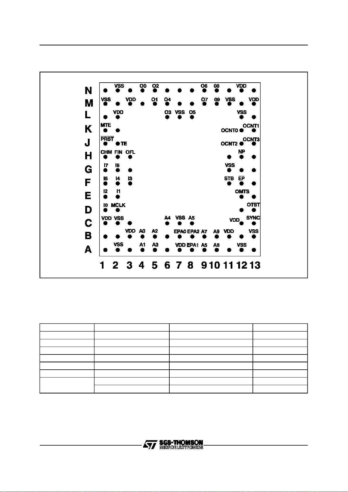
Figure2. CPGA100 PinConfiguration
2/19
W.A.R.P.1.1
VSS
VDD
MCLK
I0
I1
I2
I3
I4
I5
I6
I7
CHM
FIN
OFL
PRST
TE
MTE
VSS
VDD
VSS
VDD
O0O1O2O3O4
VSS
O5O6O7O8O9
VDD
VSS
VDD
VSSA0A1A2A3A4VDD
VSS
EPA0
EPA1
EPA2A5A6A7A8A9VDD
VSS
VDD
VSS
SYNC
OTST
OMTS
STB
EP
VSS
NP
OCNT3
OCNT2
OCNT1
OCNT0
VSS
VDD
74
73
72
71
70
69
68
67
66
65
64
63
62
61
60
59
58
57
56
55
54
33 34 35 36 37 38 39 40 41 42 43 44 45 46 47 48 49 50 51 52 53
12
13
14
15
16
17
18
19
20
21
22
23
24
25
26
27
28
29
30
31
32
11 10 9 8 7 6 5 4 3 2 1 84 83 82 81 80 79 78 77 76 75
W.A.R.P. 1.1
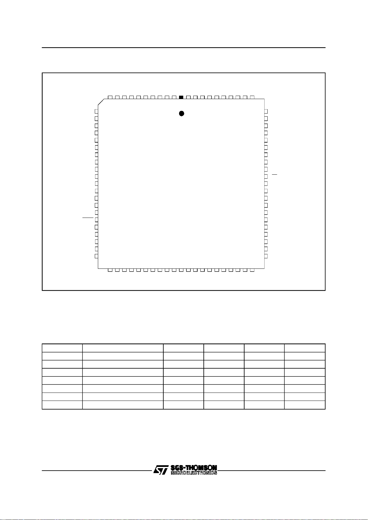
Figure3. PLCC84Pin Configuration
Symbol Parameter Min Typ Max Unit
V
DD
Supply Voltage 4.75 5.0 5.25 V
V
IL
Input Voltage 0.8 V
V
IH
Input Voltage 2 V
V
OL
Ouput Voltage 0.5 V
V
OH
Ouput Voltage 2.4 V
FCLK Clock Frequency 40 MHz
CL Output Load Capacitance 10 85 pF
Table 3. RecomendedOperationConditions (Ta=0to +70 °Cunless otherwisespecified)
3/19
W.A.R.P.1.1

Functionsindedicatedmemoriesinorderto reduce
the computationaltime. Thereforea great amount
of W.A.R.P. processing isbased on a look-uptable
approachrather than on on-linecalculation.
Those Membership Functions (MFs), each one
portrayed by a configurable resolution of 2
6
or 2
7
elements,arestored in fourinternalRAMs(1Kbyte
each). The consequentMFs, due to the different
modelling, are loaded in a single RAM by storing
for each MFitsareaandits barycentre.Thisis due
to theadoptionof theCenterofGravitydefuzzification method.
The downloading phase allows the setting of the
device, in terms of I/O number, universes of discourseandMF shapes.DuringthisphaseW.A.R.P.
prepares its internal memories for the on-line
elaboration phase and loads the microcode in its
programmemory. Thismicrocode,whichdrivesthe
on-line phase, is generated by the Compiler (see
W.A.R.P.-SDT User Manual) according to the
adoptedconfiguration.Thepossibleconfigurations
areshown in table 1.
During the on-line phase (up to 40MHz working
frequency),W.A.R.P.processes theinputdataand
producesitsoutputsaccordingtotheconfiguration
loadedin the downloadingphase.
W.A.R.P. is conceivedto work together with tradi-
Name Pins Type Function
V
DD
- Power Supply
V
SS
- Ground
A0-A9 I/O Memory Address Bus
I0-I7 I Data Input Bus
PRST I Preset
FIN I FirstInput Signal
OFL I Off-Line/On-Line Switch
CHM I ChargeMode Switch
TE I Testing(it must be connected to V
SS
)
MTE I Testing (it must be connected to V
SS
)
MCLK I Clock (up to 40 MHz)
EPA0-EPA2
*
O EPROM Address Bus
O0-O9 O Defuzzified Output
OCNT0-OCNT3 O Output Counter
STB O Strobe(Output Ready Signal)
EP O End Process
NP O New Process
OTST O Testing(it mustbe connected toV
SS
)
OMTS O Testing (it must be connected to V
SS
)
SYNC O External Synchronization
Table4. Pin Description
tional microcontrollers which shall perform normal
control tasks while W.A.R.P. will be indipendently
responsiblefor all the fuzzyrelated computing.
W.A.R.P. is manufacturedusing the high performance, reliable HCMOS4T (O.7µm) SGS-THOMSON Microelectronicsprocess.
PIN DESCRIPTION
V
DD,VSS
: Power is supplied to W.A.R.P. using
these pins.V
DD
isthe powerconnectionandVSSis
the ground connection;multi-connectionsare necessary.
A0-A9: When the CHM pin is low theyaccept as
input theaddressesfortheinternalmemory bus. In
the off-linemodetheyareusedtoaddressW.A.R.P.
memories where the microprogram and data of
antecedentandconsequentmembershipfunctions
must be loaded.
Each A0-A9 word is composed by assemblingthe
datacontainedinthe memorysupportrelatedto.cs
and .addfiles (seeW.A.R.P.-SDT User Manual).In
particular,couplesofdatarespectivelycomingfrom
.cs and .addfiles are joined to forma single A0-A9
word in the followingway:
*
Pins not usedin W.A.R.P. 1.0
4/19
W.A.R.P.1.1

A0
This resultingword allows to identifythe appropriate memory [cs2-cs0] and its respective address
[add6-add0] where the relative I0-I7 are to be
stored.
When the CHM pin is high, during the off-line
phase, W.A.R.P. generates the addresses for its
internalmemoriesandsendthoseaddressestothe
single external memory support where data (.dat
file)are located.These addresses,whichare sent
by means of the EPA0-EPA2 and A0-A9 (EPA0
MSB, A9 LSB) output pins, allow to identify the
data (on the EPROM) that have be loaded in
W.A.R.P. internalmemories.
In on-linemode A0-A9 are not used.
I0-I7: During the off-line phase these 8 data input
pins accept the microcode configuration and data
to be written into the internalmemories. The antecedentmemoryword size is 64 bits, so it is necessary to giveeachword8 bitsat a time. Inthe same
way are written the words of consequentmemory
and of program memory.
In on-linemode this bus carries the inputvariables
to W.A.R.P..Input values havea resolution of6 or
7 bits in accordancewith the configurationsetting.
PRST: This is the restart pin of W.A.R.P.. It is
possibletorestartthework during thecomputation
(on-line phase) or before the writing of internal
memories(off-linephase).In both casesit mustbe
put low at leastfora clock period.
FIN: During the on-line phase it will start the runtime acquisition cycle. This pin is activated by
providinga positivepulse fora time no lower than
an entire clock period. When all expected inputs
have been processed, a new FIN pulse must be
sent to activate a new process.
OFL: When this pin is high, the chip is enabled to
load data in the internal RAMs (off-line phase). It
mustbelowwhenthe fuzzycontrolleris waitingfor
input valuesand during the processingphase(online phase).
CHM:Thispin,whichisusedonlyduringtheoff-line
phase, determines the charge mode. CHM is not
presentin W.A.R.P.1.0 release.
When CHM is low the addresses of the internal
memory locations where data have to be stored
must be sent to W.A.R.P. from the outside by
means of the input pins A0-A9.
WhenCHM is high W.A.R.P. automaticallygenerates the addresses of its internal memories and
manages the EPROMs reading by means of the
addresses contained in EPA0-EPA2 and A0-A9
output pins(13 bits).
TE: Fortesting purpose only. It mustbeconnected
to V
SS
.
MTE: For testing purpose only. It must be connected to V
SS
.
MCLK: This is the input master clock whose frequencycan reach up to 40MHz (MAX).
During the off-line phase with CHM high, the
DCLKsignalwith a frequencyofMCLK/32 is generated in order to drive the downloading phase
timing.
EPA0-EPA2: During the off-linephase and in correspondencewithCHM high,theseoutputpins are
joined (as MSB) to A0-A9 to obtainethe complete
address ofthe memory supportwhere to read the
data to be loadedin W.A.R.P.internal memories.
EPA0-EPA2 are not used when CHM is low or in
W.A.R.P. 1.0 release.
O0-O9: These pins carry out the output values.
When the STB (strobe pin) is high, one output
variablecan bereadbyexternaldevices(in on-line
mode). The resolution ofoutput variables is 1024
points(10 bits). Ifthere are more than oneoutput,
the outputvariables are calculatedone by one and
theyare providedin the sequencestabilizedduring
the editing phase (see W.A.R.P.-SDTUser Manual).
OCNT0-OCNT3:This4 bit outputbus provides the
output variableswith a progressive number during
the on-line phase. As a consequenceit ispossible
to know towhichvariablecorrespondthedatathat
areonthe outputdatabus(O0-O9).Thedimension
of OCNT bus is connected with the maximum
number ofoutput variables (16).
STB:The strobepin enables the user to utilize the
output.When thispinishigh itindicatesthat a new
output variablehasbeen calculated andit is ready
on the output bus (O0-O9). This signal synchronizes the external devices and in particular the
interfaces with the controlled processes (on-line
mode).
EP: This signal low indicates that the processing
of all the rules has been completed.
NP: This output pin indicates that a new process
can start. NP is automatically set low before the
lastoutputhasbeencalculated,sothatitispossible
to start a new data acquisitionbefore(with a new
FIN) the computation is terminated.
A9
cs7 cs6 cs5 cs4 cs3 cs2 cs1 cs0
cs2 cs1 cs0 add6 add5 add4 add3 add2 add1 add0
add7 add6 add5 add4 add3 add2 add1 add0
5/19
W.A.R.P.1.1
OTST: For testing purpose only. It must be con-
nectedto V
SS
.
OMTS: For testing purpose only. It must be connectedto V
SS
.
SYNC:W.A.R.P. uses this pin to synchronizeinput
data from an external database in off-line mode.
The database contains informationabout antecedent and consequent membership functions and
aboutfuzzy rules. Tomemorize this database it is
possibleto use an host processor or a non volatile
memory.
FUNCTIONAL DESCRIPTION
W.A.R.P.worksintwomodedependingontheOFL
controlsignal level:
Off-line MODE (OFL High)
On-line MODE (OFLLow)
OFF-LINE MODE
All W.A.R.P. memories are loaded during the offline phase. The membershipfunctions arewritten
insidetheirrelatedmemoriesandtheprocess control rules are loaded inside the program memory.
If the CHM switch has been set low then the
addressesof the words to be written in the memories are providedby an externalbus (A0-A9), while
data must be loaded 8 bita time in the data bus.
If the CHM switch has been set high then the
addressesof the words to be written in the memories are internally generated while the addresses
of the EPROM’s locations to be read are directly
Numbers ofInput Data Resolution
Number ofMembership Functions
for TermSet
1 128 (7bit) 16
2
*
128 (7bit) 8
264(6bit)16
3 64 (6 bit) 2x8 + 1x16
464(6bit)8
*
Thisconfiguration is not available in W.A.R.P.1.0.
Table 5. AvailableConfigurations on a Single Antecedent Memory.
Figure4. Block Diagram
6/19
W.A.R.P.1.1
 Loading...