

SGS Thomson Microelectronics STE48NM50 Datasheet
STE48NM50
N-CHANNEL 500V - 0.08Ω - 48A ISOTOP
MDmesh™Power MOSFET
TYPE V
STE48NM50 500V < 0.1Ω 48 A
n
TYPICAL RDS(on) = 0.08Ω
n
HIGH dv/dt AND AVALANCHE CAPABILITIES
n
100% AVALANCHE TESTED
n
LOW INPUT CAPACITANCE AND GATE
DSS
R
DS(on)
I
D
CHARGE
n
LOW GATE INPUT RESIST ANC E
n
TIGHT PROCESS CONTROL AND HIGH
MANUFACTURING YIELDS
DESCRIPTION
The MDmesh™
is a new revolutionary MOSFET
technology that associates the Multiple Drain process with the Company’s PowerMESH™ horizontal
layout. The resulting product has an outstanding low
on-resistance, impressively high dv/dt and excellent
avalanche characteristics. The adoption of the
Company’s proprietary strip technique yields overall
dynamic performance that is significantly better than
that of similar competition’s products.
APPLICATIONS
The MDmesh™ family is very suitable for increasing
power density of high voltage converters allowing
system miniaturization and higher efficiencies.
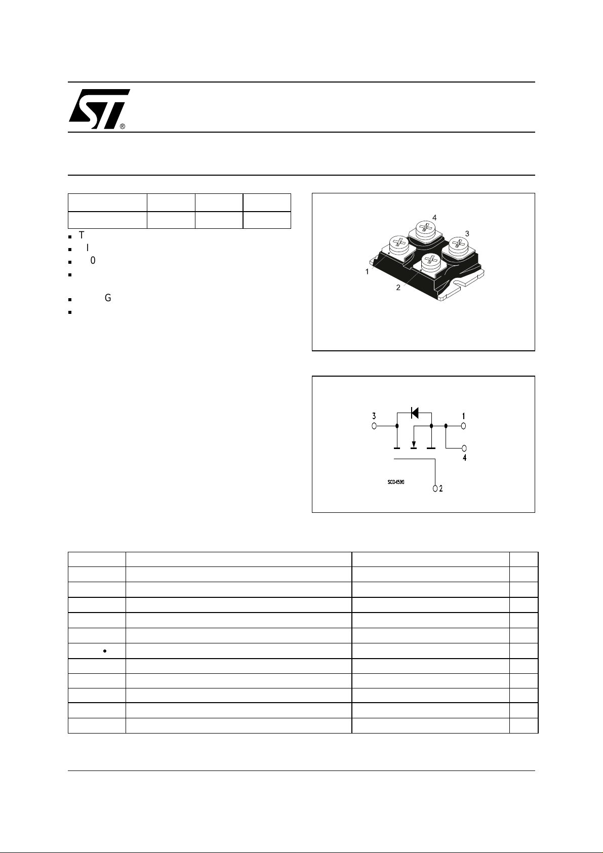
ISOTOP
INTERNAL SCHEMATIC DIAGRAM
ABSOLUTE MAXIMUM RATINGS
Symbol Parameter Value Unit
V
DS
V
DGR
V
GS
I
D
I
D
I
DM
P
TOT
dv/dt (1) Peak Diode Recovery voltage slope 15 V/ns
T
stg
T
j
(•)Pu l se width limited by safe operating area
Drain-source Voltage (VGS = 0)
Drain-gate Voltage (RGS = 20 kΩ)
Gate- source Voltage ±30 V
Drain Current (continuous) at TC = 25°C
Drain Current (continuous) at TC = 100°C
(l)
Drain Current (pulsed) 192 A
Total Dissipation at TC = 25°C
Derating Factor 3.6 W/°C
Storage Temperature –65 to 150 °C
Max. Operating Junction Temperature 150 °C
(1) ISD ≤48A, di/dt ≤400A/µs, VDD ≤ V
500 V
500 V
48 A
30 A
450 W
, Tj ≤ T
(BR)DSS
JMAX.
1/8September 2002
STE48NM50
THERMA L D ATA
Rthj-case Thermal Resistance Junction-case Max 0.28 °C/W
Rthc-sink (*) Thermal Resistance Case-sink Typ 0.05 °C/W
(*) with conductive GREASE Appli e s
AVALANCHE CHARACTERISTICS
Symbol Parameter Max Value Unit
I
AR
E
AS
Avalanche Current, Repetitive or Not-Repetitive
(pulse width limited by T
max)
j
Single Pulse Avalanche Energy
(starting T
= 25 °C, ID = IAR, VDD = 50 V)
j
15 A
810 mJ
ELECTRICAL CHARACTERISTICS (T
= 25 °C UNLESS OTHERWISE SPECIFIED)
CASE
OFF
Symbol Parameter Test Conditions Min. Typ. Max. Unit
V
(BR)DSS
Drain-source
ID = 250 µA, VGS = 0 500 V
Breakdown Voltage
V
= Max Rating
DS
VDS = Max Rating, TC = 125 °C
V
= ± 30V ±100 nA
GS
10 µA
100 µA
ON
I
I
GSS
(1)
DSS
Zero Gate Voltage
Drain Current (V
GS
Gate-body Leakage
Current (V
DS
= 0)
= 0)
Symbol Parameter Test Conditions Min. Typ. Max. Unit
V
V
GS(th)
R
DS(on)
Gate Threshold Voltage
Static Drain-source On
= VGS, ID = 250µA
DS
VGS = 10V, ID = 24A
345V
0.08 0.1 Ω
Resistance
DYNAMIC
Symbol Parameter Test Conditions Min. Typ. Max. Unit
(1) Forward Transconductance VDS > I
g
fs
ID= 24A
C
iss
C
oss
C
rss
Input Capacitance
Output Capacitance 610 pF
Reverse Transfer
V
Capacitance
R
G
Gate Input Resistance f=1 MHz Gate DC Bias = 0
Test Signal Level = 20mV
Open Drain
Note: 1. Pulsed: Pu l se duration = 300 µs, duty c ycle 1.5 %.
DS
D(on)
x R
DS(on)max,
= 25V, f = 1 MHz, VGS = 0
20 S
3700 pF
50 pF
1.7 Ω
2/8
STE48NM50
ELECTRICAL CHARACTERISTICS (CONTINUED)
SWITCHING ON
Symbol Parameter Test Conditions Min. Typ. Max. Unit
V
t
d(on)
Q
Q
Q
t
r
g
gs
gd
Turn-on Delay Time
Rise Time 35 ns
Total Gate Charge
Gate-Source Charge 23 nC
Gate-Drain Charge 42 nC
SWITCHING OFF
Symbol Param eter Test Conditions Min. Typ. Max. Unit
t
r(Voff)
t
t
f
c
Off-voltage Rise Time
Fall Time 23 ns
Cross-over Time 44 ns
SOURCE DRAIN DIODE
Symbol Parameter Test Conditions Min. Typ. Max. Unit
I
SD
I
SDM
VSD (1)
t
rr
Q
rr
I
rrm
t
rr
Q
rr
I
rrm
Note: 1. Pulsed: Pulse duration = 300 µs, duty cycle 1.5 %.
2. Pulse width limi ted by safe operating area.
(2)
Source-drain Current 48 A
Source-drain Current (pulsed) 192 A
Forward On Voltage
Reverse Recovery Time
Reverse Recovery Charg e
Reverse Recovery Curren t
Reverse Recovery Time
Reverse Recovery Charg e
Reverse Recovery Curren t
= 250V, ID = 24 A
DD
RG= 4.7Ω VGS = 10 V
(see test circuit, Figure 3)
V
= 400 V, ID = 48 A,
DD
V
= 10 V
GS
V
= 400 V, ID = 48 A,
DD
RG= 4.7Ω, V
GS
= 10 V
(see test circuit, Figure 5)
ISD = 48 A, VGS = 0
= 40 A, di/dt = 100A/µs,
I
SD
V
= 100 V, Tj = 25°C
DD
(see test circuit, Figure 5)
= 40 A, di/dt = 100A/µs,
I
SD
VDD = 100 V, Tj = 150°C
(see test circuit, Figure 5)
40 ns
87 117 nC
18 ns
1.5 V
520
7.8
30
680
11.2
33
ns
µC
A
ns
µC
A
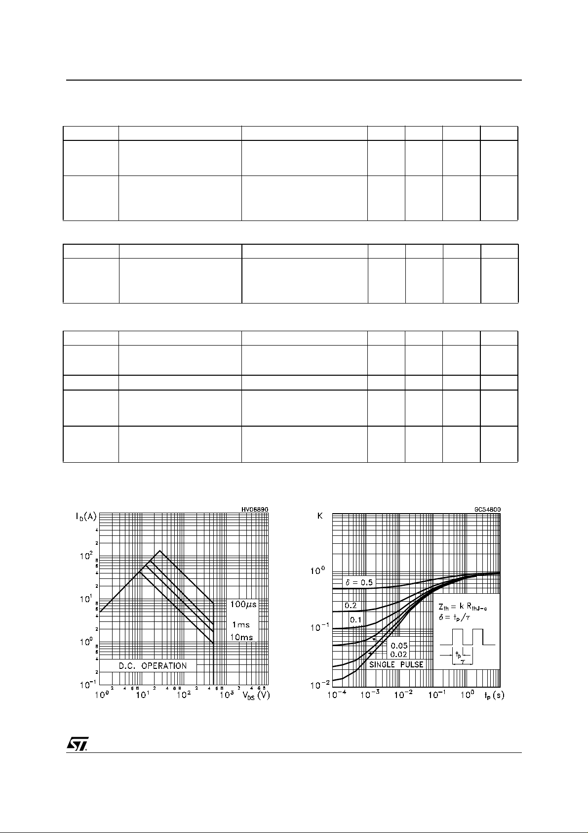
Thermal ImpedenceSafe Operating Area
3/8
 Loading...