

SGS Thomson Microelectronics STE40NA60 Datasheet
N - CHANNEL ENHANCEMENT MODE
FAST POWER MOS TRANSISTOR
TYPE V
DSS
STE40 NA 6 0 600 V < 0 .135 Ω 40 A
R
DS(on)
I
D
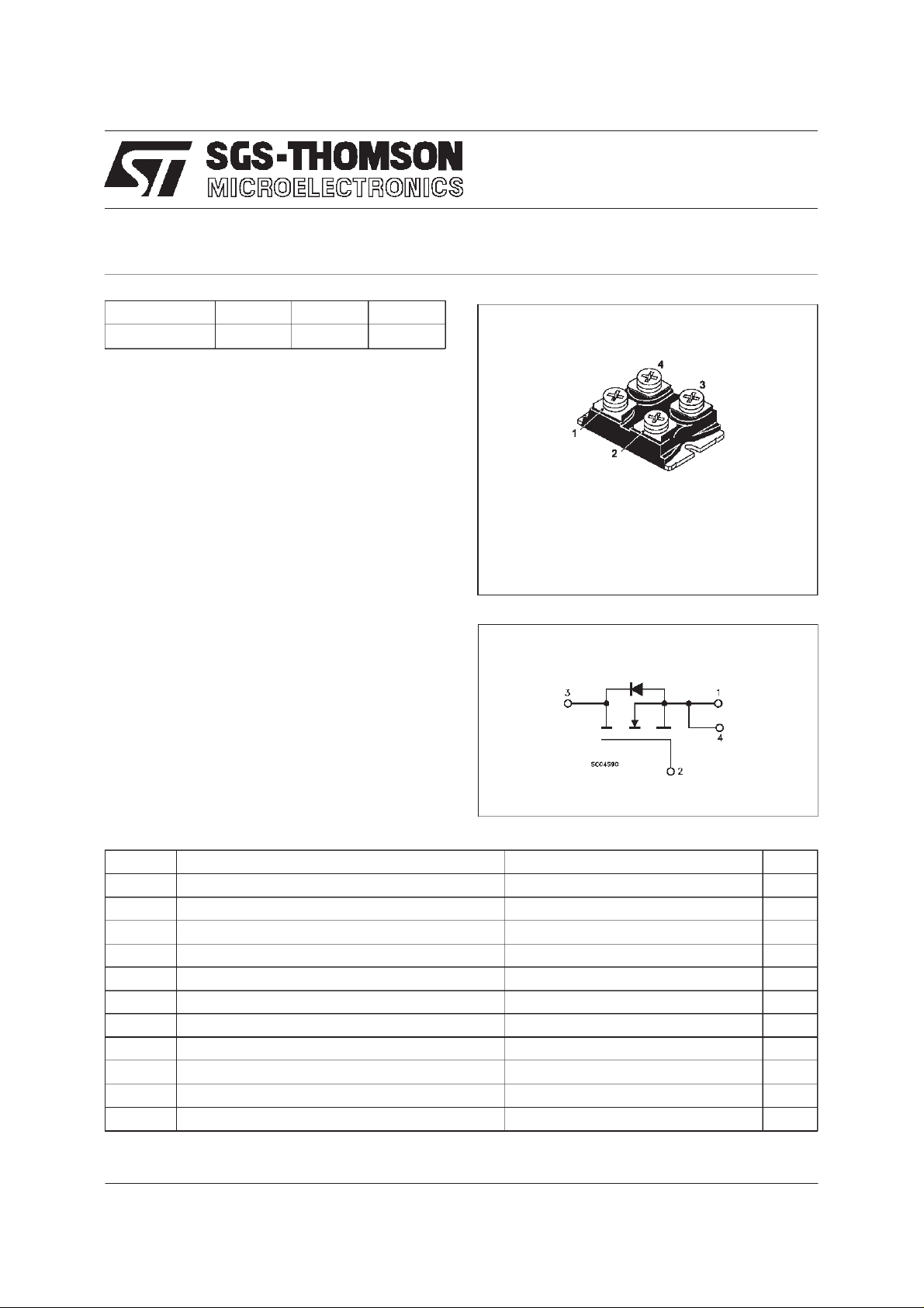
STE40NA60
PRELIMINARY DATA
■ TYPICALR
■ HIGH CURRENTPOWER MODULE
■ AVALANCHERUGGEDTECHNOLOGY
■ VERYLARGE SOA - LARGE PEAK POWER
DS(on)
=0.12 Ω
CAPABILITY
■ EASY TO MOUNT
■ SAME CURRENTCAPABILITYFOR THE
TWOSOURCE TERMINALS
■ EXTREMELY LOW Rth (Junctionto case)
■ VERYLOW INTERNAL PARASITIC
INDUCTANCE
■ ISOLATEDPACKAGEULRECOGNIZED
APPLICATIONS
■ SMPS & UPS
■ MOTORCONTROL
■ WELDINGEQUIPMENT
■ OUTPUTSTAGE FOR PWM,ULTRASONIC
CIRCUITS
ISOTOP
INTERNAL SCHEMATIC DIAGRAM
ABSOLUTE MAXIMUM RATINGS
Symbol Parameter Value Unit
V
V
V
I
DM
P
T
V
(•) Pulsewidth limited by safe operatingarea
January 1998
Drain-sourc e V ol t ag e (VGS=0) 600 V
DS
Drain- g at e Voltage (RGS=20kΩ)
DGR
Gate- source Voltage ± 30 V
GS
I
Drain Current (con t inuous) a t Tc=25oC40A
D
I
Drain Current (con t inuous) a t Tc=100oC26A
D
600 V
(•) Drain Current (pulsed) 160 A
Total Dissipation at Tc=25oC460W
tot
Derating Factor 3.6 W/
St orage Temperatur e -55 to 15 0
stg
T
Max. Operating Junction T empe rature 150
j
Insulation Withhstand Voltage (AC-RMS) 2500 V
ISO
o
C
o
C
o
C
1/5
STE40NA60
THERMAL DATA
R
thj-case
R
thc-h
AVALANCHE CHARACTERISTICS
Symbol Para met e r Max Value Uni t
I
AR
E
Ther mal Resist ance Junctio n-case Max
Ther mal Resist ance Case-heat si nk With C ond uctive
Gr ease A p plied M ax
Avalanche Cur rent, Repet it i v e or Not-Re petitive
(pulse width lim ited b y T
Single Pulse Avalanche Energy
AS
(starting T
=25oC, ID=IAR,VDD=50V)
j
max, δ <1%)
j
0.27
0.05
20 A
3000 mJ
o
C/W
o
C/W
ELECTRICAL CHARACTERISTICS (T
=25oC unlessotherwise specified)
case
OFF
Symbol Parameter Test Cond itions Min. Typ. Max. Unit
V
(BR)DSS
Drain-sourc e
=500µAVGS=0
I
D
900 V
Breakdown V oltage
I
I
DSS
GSS
Zer o Gat e V o lt age
Drain Current (V
GS
Gat e-body Leaka ge
Current (V
DS
=0)
=0)
V
=MaxRating
DS
=0.8x Max Rating Tc= 125oC
V
DS
= ± 30 V
V
GS
250
1000µAµA
± 200 nA
ON (∗)
Symbol Parameter Test Cond itions Min. Typ. Max. Unit
V
GS(th )
Gate Threshold
VDS=VGSID=1mA 2.25 3 3.75 V
Voltage
R
DS(on)
Stati c D rain-source On
VGS=10V ID= 2 0 A 0.12 0. 1 35 Ω
Resistance
I
D(on)
On State Drain Curre nt VDS>I
D(on)xRDS(on)max
40 A
VGS=10V
DYNAMIC
Symbol Parameter Test Cond itions Min. Typ. Max. Unit
g
(∗)Forward
fs
Tr ansconductanc e
C
C
C
Input Capac i t an c e
iss
Out put C apa c itance
oss
Reverse Transf er
rss
Capa cit an c e
VDS>I
D(on)xRDS(on)maxID
=20A 20 S
VDS=25V f=1.0MHz VGS= 0 13000
1500
350
16000
1700
450
pF
pF
pF
2/5
 Loading...