

SGS Thomson Microelectronics STE24NA100 Datasheet
STE24NA100
N - CHANNEL 1000V - 0.35Ω - 24A - ISOTOP
FAST POWER MOSFET
TYPE V
DSS
R
DS(on)
I
D
ST E24NA100 1000 V < 0. 385 Ω 24 A
■ TYPICALR
30V GATE TO SOURCE VOLTAGERATING
■
±
■ 100%AVALANCHETESTED
■ LOW INTRINSICCAPACITANCE
■ GATECHARGE MINIMIZED
■ REDUCEDVOLTAGESPREAD
DS(on)
= 0.35 Ω
APPLICATIONS
■ HIGHCURRENT, HIGH SPEED SWITCHING
■ SWITCHMODE POWER SUPPLY (SMPS)
■ DC-AC CONVERTERFOR WELDING
EQUIPMENTANDUNINTERRUPTABLE
POWERSUPPLY AND MOTOR DRIVE
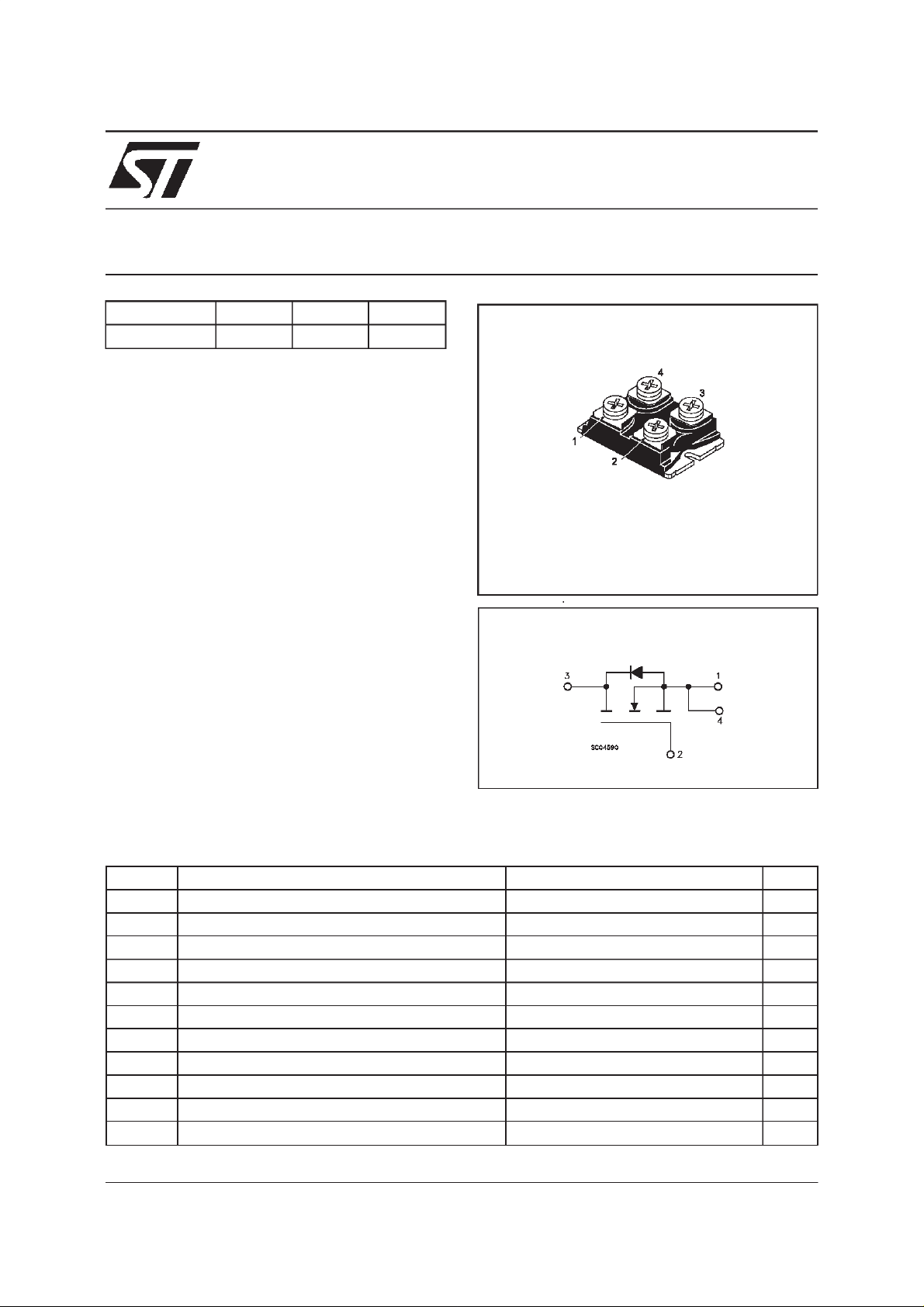
ISOTOP
INTERNAL SCHEMATIC DIAGRAM
ABSOLUTE MAXIMUM RATINGS
Symb o l Parameter Value Unit
V
V
V
I
DM
P
T
V
(•) Pulsewidth limited by safeoperating area
October 1998
Drain-source Voltage (VGS= 0) 1000 V
DS
Drain- g at e V olt ag e (RGS=20kΩ) 1000 V
DGR
Gate-s ource Voltage
GS
I
Drain Cur rent (cont inu ous ) at Tc=25oC24A
D
I
Drain Cur rent (cont inu ous ) at Tc=100oC15A
D
30 V
±
(•) Drain Cur rent (pulsed) 96 A
Tot al Dissi pat ion at Tc=25oC 450 W
tot
Derat ing F ac tor 3.6 W/
Sto rage Temperat ure -55 to 150
stg
T
Max. Operating J unction T emperat ure 150
j
Ins ulat i on Wi t hs t an d V olt ag e (AC- RMS) 2500 V
ISO
o
C
o
C
o
C
1/8
STE24NA100
THERMAL DATA
R
thj-case
R
thc-h
AVALANCHE CHARACTERISTICS
Symbol Parameter Max Valu e Unit
I
AR
E
Ther mal Resistanc e Junct ion-case Max
Ther mal Resistanc e Case-heatsink Wit h C onductive
Gr ease Applied Max
Avalanche Current, Repetitive or Not-Repetitive
(pulse width limited by T
Single Pul se A v alan c he Ener gy
AS
(starting T
=25oC, ID=IAR,VDD=50V)
j
max)
j
0.27
0.05
12 A
2000 mJ
o
C/W
o
C/W
ELECTRICAL CHARACTERISTICS
=25oC unless otherwisespecified)
(T
case
OFF
Symbol Parameter Test Conditions Min. Typ. M ax. Unit
V
(BR)DSS
Drain-source
ID=500µAVGS= 0 1000 V
Break dow n Vo lt age
I
DSS
I
GSS
Zero Gate Voltage
Drain Curre nt (V
GS
Gat e- bod y Leakag e
Current (V
DS
=0)
=0)
V
=MaxRating
DS
=MaxRating Tc= 125oC
V
DS
= ± 30 V ± 400 nA
V
GS
50
250
ON(∗)
Symbol Parameter Test Conditions Min. Typ. M ax. Unit
V
GS(th)
R
DS(on)
Gate Threshold Voltage VDS=V
Sta t ic Drain-s our c e On
VGS=10V ID= 12 A 0.35 0 . 385 Ω
GS
ID=1mA 2.25 3 3.75 V
Resistance
I
D(on)
On State Drain Current VDS>I
D(on)xRDS(on )max
24 A
VGS=10V
DYNAMIC
Symbol Parameter Test Conditions Min. Typ. M ax. Unit
g
(∗)Forward
fs
Tr ansc on duc tance
C
C
C
Input Capacitanc e
iss
Out put Capac itance
oss
Reverse Transfer
rss
Capacit a nc e
VDS>I
D(on)xRDS(on )max
ID=12A 15 S
VDS=25V f=1MHz VGS=0 14000
1200
300
19000
1600
390
µA
µ
pF
pF
pF
A
2/8
STE24NA100
ELECTRICAL CHARACTERISTICS
(continued)
SWITCHINGON
Symbol Parameter Test Conditions Min. Typ. M ax. Unit
t
d(on)
t
r
Turn-on Time
Rise T i m e
VDD=500V ID=12A
R
=4.7
G
Ω
VGS=10V
40
55
56
77
(see test circuit, figure 3)
Q
Q
Q
Tot al Gate Charge
g
Gat e- Source Char g e
gs
Gate-Drain Charge
gd
VDD= 800 V ID=24A VGS= 10 V 470
43
226
660 nC
SWITCHINGOFF
Symbol Parameter Test Conditions Min. Typ. M ax. Unit
t
r(Voff)
t
t
Off-volt age Rise Time
Fall T ime
f
Cross-over Tim e
c
VDD=800V ID=24A
=4.7 Ω VGS=10V
R
G
(see test circuit, figure 5)
110
25
150
154
35
210
SOURCEDRAINDIODE
Symbol Parameter Test Conditions Min. Typ. M ax. Unit
I
SDM
V
I
SD
Q
I
RRM
SD
t
Source-drain Current
(•)
Source-drain Current
24
96
(pulsed)
(∗)ForwardOnVoltage ISD=24A VGS=0 1.6 V
Reverse Recovery
rr
Time
Reverse Recovery
rr
ISD= 24 A di/dt = 100 A/µs
= 100 V Tj=150oC
V
DD
(see test circuit, figure 5)
1.4
41
Charge
Reverse Recovery
60
Current
ns
ns
nC
nC
ns
ns
ns
A
A
µ
µ
A
s
C
(∗) Pulsed:Pulse duration = 300µs, duty cycle 1.5%
(•) Pulse width limited by safeoperating area
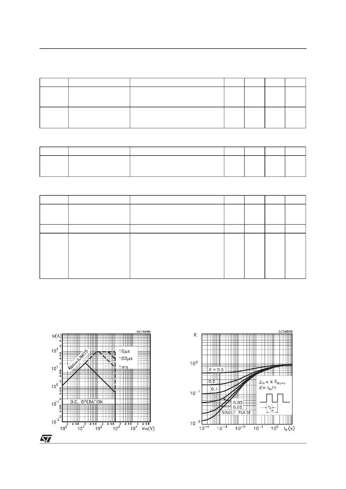
SafeOperating Area Thermal Impedance
3/8
 Loading...