STE2002
81 X 128 SINGLE CHIP LCD CONTROLLER / DRIVER
■ 104 x 128 bits Display Data RAM
■ Programmable MUX rate
■ Programmable Frame Rate
■ X,Y Programmable Carriage Return
■ Dual Partial Display Mode
■ Row by Row Scrolling
■ Automatic data RAM Blanking procedure
■ Selectable Input Interface:
2
• I
C Bus Fast and Hs-mode (read and write)
• Parallel Interface (read and write)
• Serial Interface (read and write)
■ Fully Integrated Oscillat or requires no ex ternal
components
■ CMOS Compatible Inputs
■ Fully Integrated Configurable LCD bias voltage
generator with:
• Selectabl e
multiplication factor (up to 6X)
• Effective sensing for High Precision Output
• Eight selectable temperature compensation
coefficients
■ Designed for chip-on-glass (COG) applications
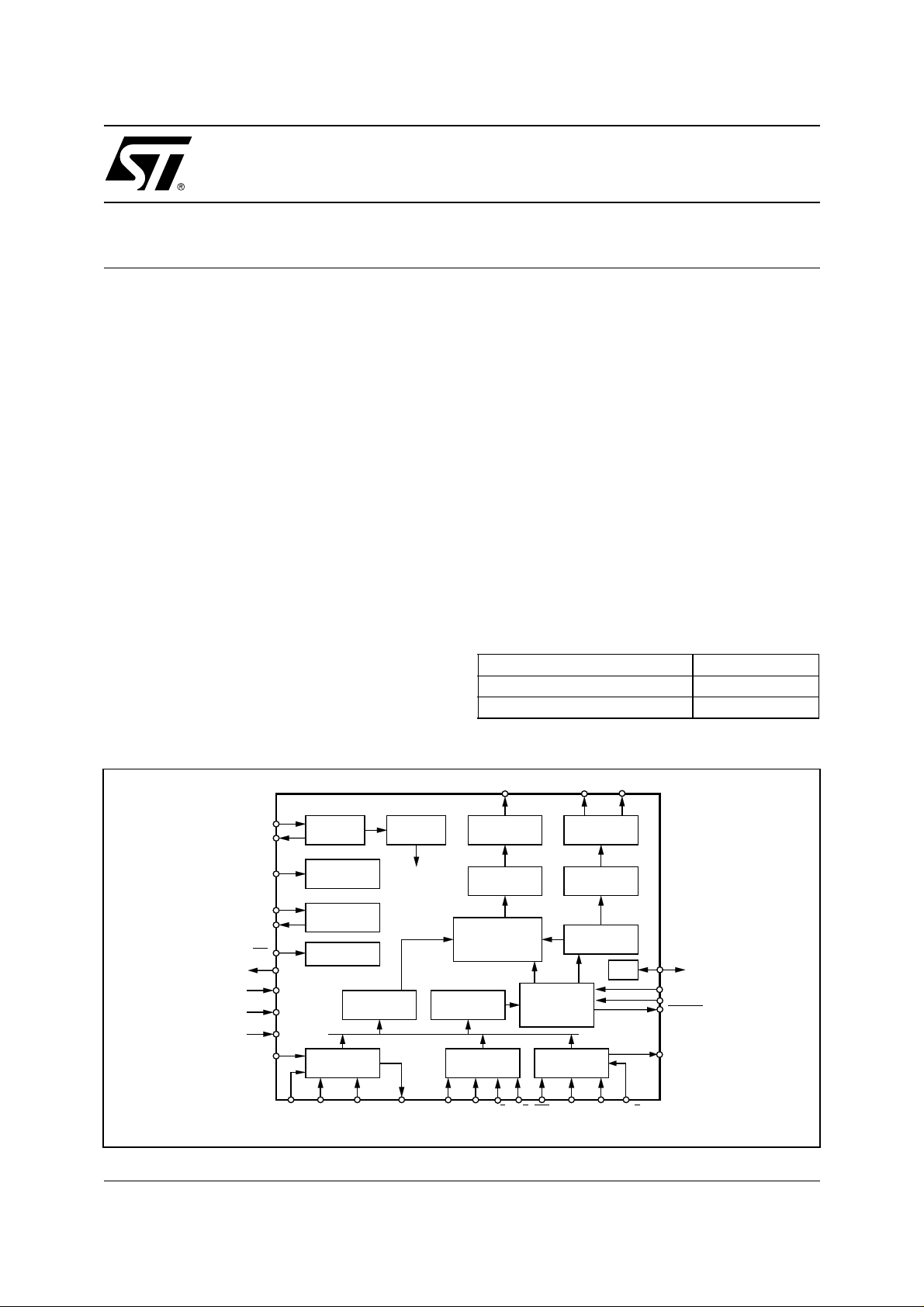
Figure 1. Block Diagram
■ Low Power Consumption, suitable for battery
operated systems
■ Logic Supply Voltage range from 1.7 to 3.6V
■ High Voltage Generator Supply Voltage range
from 1.75 to 4.2V
■ Display Supply Voltage range from 4.5 to 11V
■ Backward Compatibility with STE2001
DESCRIPTION
The STE2002 is a low power CMOS LCD controller
driver. Designed to drive a 81 rows by 128 columns
graphic display, provides all necessary functions in a
single chip, including on-chip LCD supply and bias
voltages generators, resulting in a minimum of externals components and in a very low power consumption. The STE2002 features three standard interfaces
(Seria l, P ar allel & I
host
m
controller.
Bumped Wafers STE2002DIE1
Bumped Dice on Waffle Pack
2
C) for ease of interfacing with the
Type Ordering Number
STE2002DIE2
September 2002
OSC_IN
OSC_OUT
VLCDIN
VLCDSENSE
VLCDOUT
RES
VSSAUX
VDD1,2
V
SS
SEL1,2
SA1
SAO
OSC
BIAS VOLTAGE
GENERATOR
HIGH VOLTAGE
GENERATOR
RESET
REGISTER
I2CBUS
SDA_IN SDA_OUTSCL
DATA
TIMING
GENERATOR
CLOCK
INSTRUCTION
DB0 to DB7 E PD/C
CO to C127 R0 to R80
COLUMN
DRIVERS
DATA
LATCHES
104 x 128
RAM
DISPLAY
REGISTER
PARALLEL SERIAL
CONTROL
LOGIC
SCE SDIN SCLK SD/C
R/W
ROW
DRIVERS
SHIFT
REGISTER
SCROLL
LOGIC
ICON
TEST
TEST_1_14
ICON_MODE
EXT
BSY_FLG
SOUT
1/51
STE2002
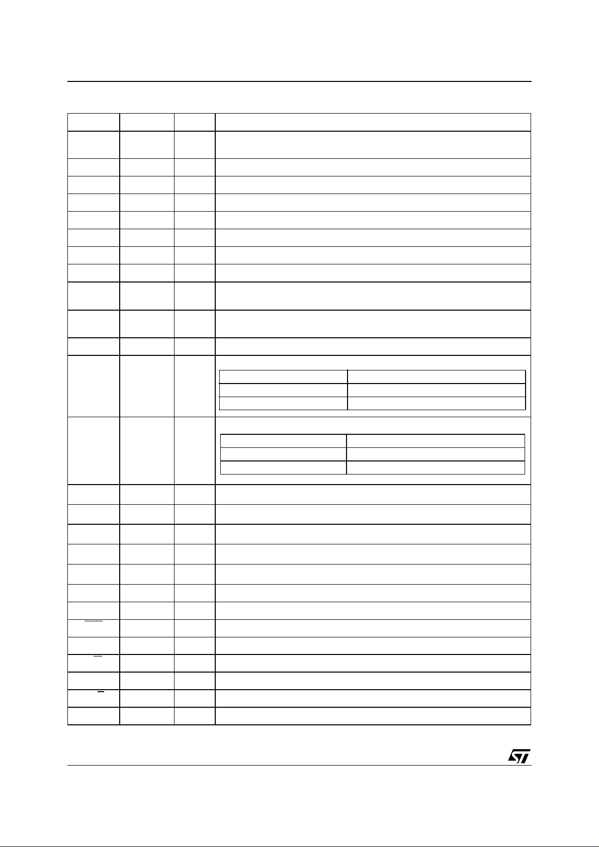
PIN DESCRIPTION
N° Pad T ype Function
R0 to R80 129-169
O LCD Row Driver Output
282-322
ICON 323 O ICON Row Driver
C0 to C127 1-128 O LCD Column Driver Output
SS 236-255 GND Ground pads.
V
DD1 188-199 Supply IC Positive Power Supply
V
DD2 200-211 Supply Internal Generator Supply Voltages.
V
LCDIN 261-270 Supply LCD Supply Voltages for the Column and Row Output Drivers.
V
VLCDOUT 273-282 Supply Voltage Multiplier Output
V
LCDSENSE
271-272 Supply Voltage Multiplier Regulation Input. V
Sensing for Output Voltage Fine
LCDOUT
Tuning
V
SSAUX
180, 231,
O Ground Reference for Selection Pins Configuration
218
SEL1,2 184,185 I Interface Mode Selection
EXT 1 83 I Extended Instruction Set Selecti on
EXT PAD CONFIG INSTRUCTION SET SELECTED
VSS or VSSAUX BASIC
VDD1 EXTENDED
ICON_MO
DE
186 I ICON ROW Management
ICON MODE PAD CONFIG ICON MODE STATUS
VSS or VSSAUX DISABLED
VDD1 ENABLED
SDA_IN 234 I
SDA_OUT 232 O
SCL 235 I
SA0 182 I
SA1 181 I
2
C Bus Data In
I
2
C Bus Data Out
I
2
C bus Clock
I
2
C Slave Address BIT 0
I
2
C Slave Address BIT 1
I
OSCIN 187 I External Oscillator Input
OSCOUT 260 O Internal/External Oscillator Out
RES
230 I Reset Input. Active Low.
DB0 to DB7 220-227 I/O Parallel Interface 8 Bit Data Bus
R/W
219 I Parallel Interface Read & Write Control Line
E 229 I Parallel Interface Data Latch Signal.
PD/C
228 I Parallel Interface Data/Command Selector
SDIN 214 I Serial Interface Data Input
2/51

STE2002
PIN DESCRIPTION
N° Pad Type Function
SCLK 217 I Serial Interface Clock
SCE
SD/C
SOUT 213 O Serial Out
BSYFLG
T1 to T14 170-179,
(continued)
216 I Serial Interface ENABLE. When Low the Incoming Data are Clocked In.
215 I Serial Interface Data/Command Selector
212 O Active Procedure Flag. Notice if There is an ongoing Internal Operation or an
active reset. Active Low.
I/O Test Pads. - A 50kohm pull-down resistor is added on input pis.
256-259
Test Num. Pin Configuration
TEST_1
TEST_2
TEST_3
TEST_4
TEST_5
TEST_6
TEST_7
TEST_8
TEST_9
TEST_10
TEST_11
TEST_12
TEST_13
TEST_14
OPEN
VSS / VSSAUX
VSS / VSSAUX
3/51
STE2002
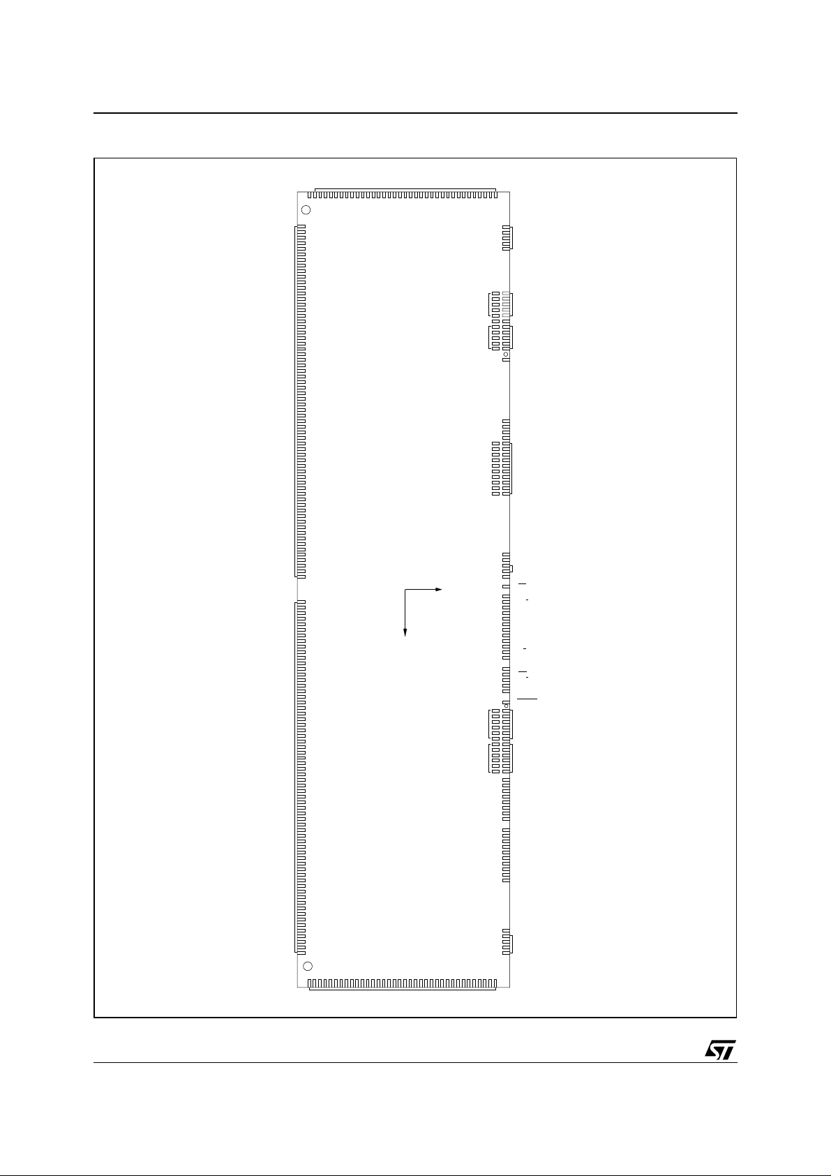
Figure 2. Chip Mechanical Drawing
COL 0
COL 63
COL 64
ROW 0
ICON
MARK_1
STE2002
(0,0)
ROW 34
ROW 35
ROW 39.
MARK_3
MARK_4
VLCDOUT
VLCDSENSE
VLCDIN
OSCOUT
TEST_14
TEST_13
TEST_12
TEST_11
VSS
SCL
SDAIN
SDAOUT
VSSAUX
RES
E
PD/C
D0
D1
D2
D3
D4
D5
D6
D7
R/W
VSSAUX
SCLK
SCE
SD/C
SDIN
SDOUT
BSY_FLG
VDD2
VLCDOUT
VLCDSENSE
VLCDIN
Y
X
VDD2
4/51
COL 127
ROW 40
MARK_2
VDD1
VDD1
OSCIN
ICON_MODE
SEL1
SEL2
EXT_SET
SA0
SA1
VSSAUX
TEST_10
TEST_9
TEST_8
TEST_7
TEST_6
TEST_5
TEST_4
TEST_3
TEST_2
TEST_1
ROW 80/ICON
ROW 79
ROW 76
ROW 75
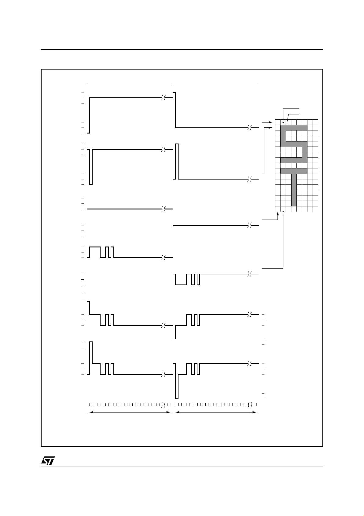
Figure 3. Improved ALTH & PLESKO Driving Method
V
LCD
V
2
V
3
ROW 0
R0 (t)
V
4
V
5
V
SS
V
LCD
V
2
V
3
ROW 1
R1 (t)
V
4
V
5
V
SS
V
LCD
V
2
V
3
COL 0
C0 (t)
V
4
V
5
V
SS
V
LCD
V
2
V
3
COL 1
C1 (t)
V
4
V
5
V
SS
V
- V
LCD
SS
V3 - V
SS
STE2002
∆V1(t)
∆V
(t)
2
V
V
state1
state2
- V
V
LCD
(t)
V3 - V
V
- V
LCD
V3 - V
- V
V
LCD
(t)
V3 - V
(t) = C1(t) - R0(t)
∆V
1
∆V
(t) = C1(t) - R1(t)
2
2
0V
SS
SS
SS
2
0V
SS
0 1 2 3 4 5 6 7 8 9 64
.......
FRAME n FRAME n + 1
0 1 2 3 4 5 6 7 8 9 64
.....
.......
.....
V
4 - V5
0V
V
SS - V5
V4 - V
VSS - V
V
4 - V5
0V
V
SS - V5
V4 - V
VSS - V
D00IN1154
LCD
LCD
LCD
LCD
5/51
STE2002
0
CIRCUIT DESCRIPTION
Supplies Voltages and Gro un ds
is supply voltages to the internal voltage generator (see below). If the internal voltage generator is
V
DD2
not used, this should be c onnected to V
could be different form V
DD2
.
Internal Supply Voltage Ge nerator
The IC has a fully integrated (no external capacitors required) charge pump for the Liquid Crystal Display
supply voltage generation. The multiplying factor can be programmed to be: Auto, X6, X5, X4, X3, X2, using the ’set CP Multiplication’ Command. If Auto is set, the multiplying factor is automatically selected to
have the lowest current consumption in every condition. This make possible to have an input voltage that
changes over time and a constant V
the V
LCDSENSE
pad. For this voltage, eight different temperature coefficients (TC, rate of change with tem-
LCD
perature) can be programmed using th e bits TC1 and TC0 and T2,T1 & T0. This will ensure no cont rast
degradation over the LCD operating range. Using the internal charge pump, the V
must be connected together. An external supply could be connected to V
using the internal generator. In such event the V
the internal voltage generator must be programmed to zero (PRS = [0;0], Vop = 0 - Reset condition).
Oscillator
A fully integrated oscillator (requires no externa l com ponen ts) is presen t to provi de t he clock f or t he Display System. When u sed the O SC pad must be connec ted to V
used and fed into the OSC pin. An oscillator out is provided on the OSCOUT Pad to cascade two or more
drivers
Bias Levels
To properly drive the LCD, six (Including VLCD and VSS) different voltage (Bias ) levels are generated.
The ratios among these levels and VLCD, s hould be selected acc ording to the MUX ratio (m). They are
established to be (Fig. 4):
DD1
pad. V
supplies the rest of the IC. V
DD1
voltage. The output voltage (V
LDCOUT
and V
LCDSENSE
DD1
supply voltage
DD1
LCDOUT
) is tightly controlled through
and V
LCDIN
to supply the LCD without
LCDIN
LCDOUT
pads
must be connected to GND and
pad. An external oscillator could be
LCD
n3+
,
------------ - V
n4+
LCD
n2+
,
------------ - V
n4+
LCD
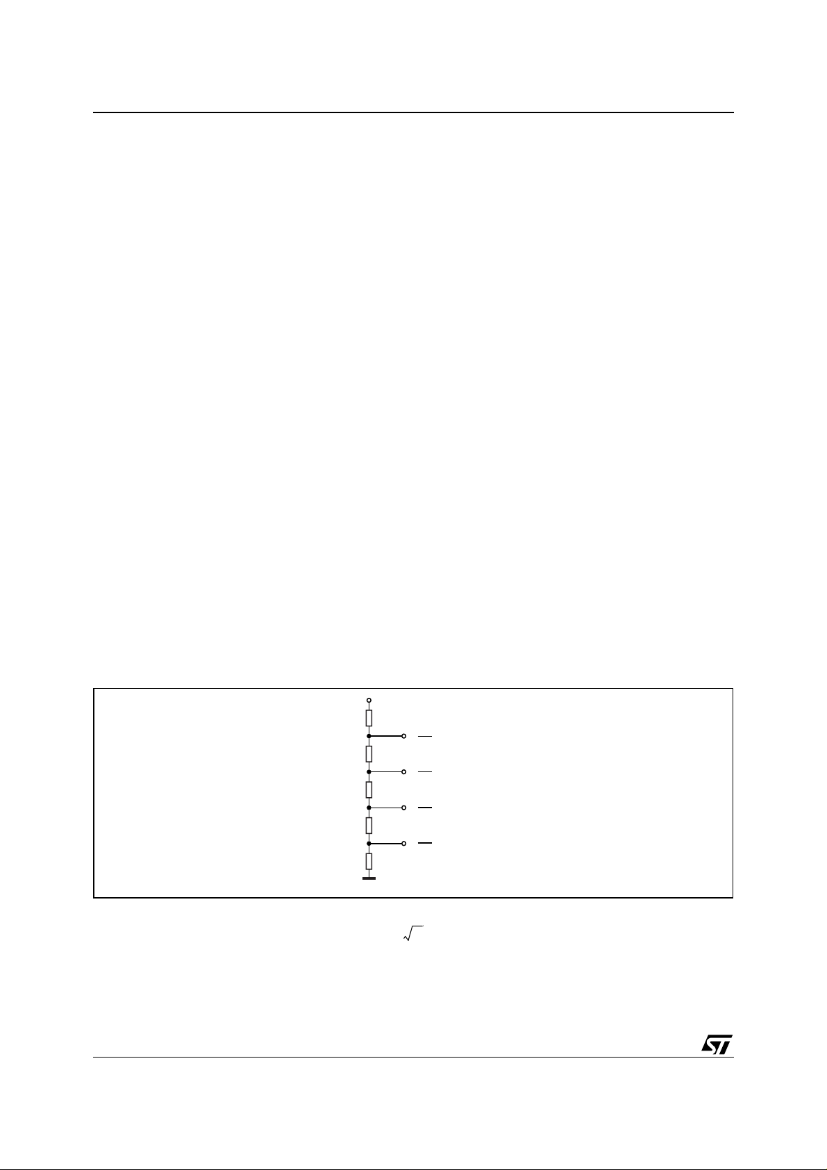
Figure 4. Bias level Generator
R
R
nR
R
R
thus providing an 1/(n+4) ratio, with n calculated from:
nm3–=
For m = 81, n = 6 and an 1/10 ratio is set.
For m = 65, n =5 and an 1/9 ratio is set.
2
,
------------ - V
n4+
V
LCD
n + 3
·V
LCD
n + 4
n + 2
·V
LCD
n + 4
2
·V
LCD
n + 4
1
·V
LCD
n + 4
V
SS
D00IN115
LCD
1
,
------------ - V
n4+
LCD,VSS
6/51

STE2002
The STE2002 provides three bits (BS0, BS1, BS2) for programming the desired Bias Ratio as shown below:
BS2 BS1 BS0 n
0007
0016
0105
0114
1003
1012
1101
1110
The following table Bias Level for m = 65 and m = 81 are provided:
Symbol m = 65 (1/9) m = 81 (1/10)
V1 V
V2 8/9*V
V3 7/9*V
V4 2/9*V V
V5 1/9 *V
V6 V
LCD
SS
LCD
LCD
LCD
LCD
V
LCD
9/10*V
8/10*V
2/10*V
1/10*V
V
SS
LCD
LCD
LCD
LCD
LCD Voltage Generation
The LCD Voltage at reference temperature (To = 27°C) can be set using the VOP register content according to
the following formula:
V
LCD
(T=To) = V
o = (Ai+VOP · B) (i=0,1,2)
LCD
with the following values:
Symbol Value Unit Note
Ao 2.95 V PRS = [0;0]
A1 6.83 V PRS = [0;1]
A2 10.71 V PRS = [1;0]
B 0.03 03 V
To 27 °C
Note that the three PRS values produce three adjacent ranges for VLCD. If the V
register and PRS bits are
OP
set to zero the internal voltage generator is switched off.
The proper value for the VLCD is a function of the Liquid Crystal Threshold Voltage (Vth) and of the Multiplexing
Rate. A general expression for this is:
1m+
----------------------------------- - V
V
LCD(to)
op
-----------------------------------------=
V
⋅=
th
1
⋅
21
-------- -–
m
= 6.85 · V
th
6.85 VthAi–⋅()
0.03
For MUX Rate m = 65 the ideal V
than:
LCD
is:
V
LCD
7/51

STE2002
Temperature Coefficient
As the viscosity, and therefore the contrast, of the LCD are subject to change with temperature, there's the need
to vary the LCD Voltage with temperature. The STE2002 provides the possibility to change the VLCD in a linear
fashion against temperature with eight different Temperature Coefficient selectable through the T2, T1 and T0
bits. Only four of them are available with basic instruction set (TC1 & TC0 Bits).
NAME TC1 TC0 Value Unit
TC0 0 0
TC2 0 1
TC3 1 0
TC6 1 1
-0.7 · 10
-1.05· 10
-2.1 · 10
-0.0· 10
-3
-3
-3
-3
NAME TC2 TC1 TC0 Value Unit
TC0 0 0 0
TC1 0 1 1
TC2 1 0 0
TC3 1 1 1
TC4 1 1 1
TC5 1 1 1
TC6 1 1 1
TC7 1 1 1
-0.35 · 10
-0.7 · 10
-1.05· 10
-1.4 · 10
-1.75· 10
-2.1 · 10
-0.0· 10
-2.3· 10
-3
-3
-3
-3
-3
-3
-3
-3
Figure 5.
1/ °C
1/°C
1/°C
1/°C
1/ °C
1/°C
1/°C
1/°C
1/°C
1/°C
1/°C
1/°C
LCD
V
0
A
00h 01h 02h 03h 04h 05h ….
Finally, the V
8/51
B
1
0
A
+ B
7Ch 7Dh 7Eh
PRS = [0;0]
voltage at a given (T) temperature can be calculated as:
LCD
A
7Fh 00h 01h 02h
(T) = V
V
LCD
03h 04h
05h …. 7Ch
PRS = [0;1]
o · [1 + (T-To) · T C]
LCD
7Dh 7Eh 7Fh
2
A
00h 01h 02h 03h 04h
05h 7Ch
….
PRS = [1;0]
7Dh 7Eh 7Fh
O
V

STE2002
Display Data RAM
The STE2002, provides an 104X128 bits Static RAM to store Display da ta. This is organized into 13
(Bank0 to Bank12) banks with 128 Bytes. One of these banks (128 bits wide) can be used for Icons. RAM
access is accomplished in either one of the Bus Interfaces provided (s ee bel ow). Allowed address es are
X0 to X127 (Horizontal) and Y0 to Y12 (Vertical).
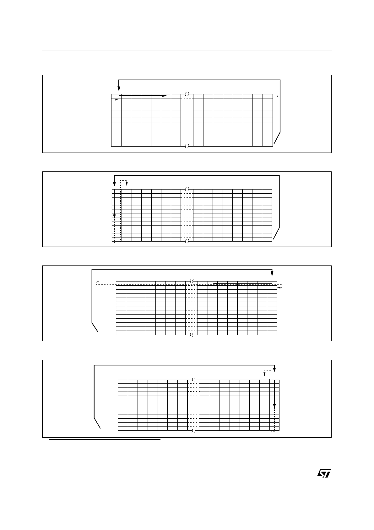
When writing to RAM, four addressing mode are provided:
• Normal Horizontal (MX=0 and V=0), having the column with address X= 0 located on the left of the memory map. The X pointer is increased after each byte written. After the last column address (X=X-Carriage), Y address pointer is set to jump to the following bank and X restarts from X=0. (Fig. 6)
• Normal Vertical (MX=0 and V=1), having the column with address X= 0 located on the left of the memory
map. The Y pointer is increased after each byte written. After th e l ast Y bank address (Y =Y-Carriage ),
X address pointer is set to jump to next column and Y restarts from Y=0 (Fig. 7).
• Mirrored Horizontal (MX=1 and V=0), having the column with address X= 0 located on the right of the
memory map. The X pointer is increased af ter each byte written. After the last column address (X=XCarriage), Y address pointer is set to jump to the next bank and X restarts from X=0 (fig. 8).
• Mirrored Vertical (MX=1 and V=1), having the column with address X= 0 located on the right of the memory map. The Y pointer is increased after each byte written. After the last Y bank address (Y=Y-Carriage), the X pointer is set to jump to next column and Y restarts from Y=0 (fig. 9).
After the last allowed address (X;Y)=(X-Carriage; Y-Carriage), the address pointers always jump to the
cell with address (X;Y) = (0;0) (Fi. 10, 11, 12 & 13).
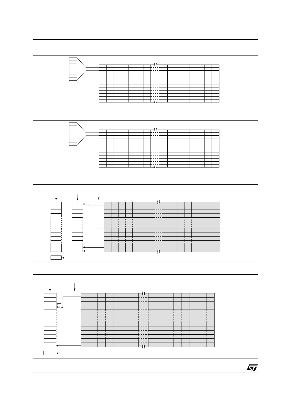
Data bytes in the memory could have the MSB either on top (D0 = 0, Fig.14) or on the bottom (D0=1, Fig.
15).
The STE2002 provides also means to alter the normal output addressing. A mirroring of the Display along
the X axis is enabled setting t o a l ogic one MY bit.This function does n't af fect t he cont ent of the me mory
RAM. It is only related to the visualization process.
When ICON MODE=1 the Icon Row is not mirrored with MY and is not scrolled. When ICON Mode=0 the
Icon Row is like the other graphic lines and is mirrored and scrolled.
Four are the multiplex ratio avai lable when the partial d isplay mode is disabled (MUX 33 , MUX 49, MUX
65 and MUX 81).
Only a subset of writable rows are output on Row drivers.
When Y-Carriage<MUX/8, if Mux 65 is selected only the first 65 m emory r ows are v isualized, if Mux 49 i s
selected only the first 49 memory rows are visualized, if Mux 33 is selected only the first 33 memory rows
are visualized. All unused Row and Column drivers must be left floating.
When Y-Carriage<MUX/8, the icon Bank i s located t o B A NK 10 in MUX 81 Mode, to BANK8 i n M U X 65
Mode, to BANK 6 in MUX 49 Mode and to BANK 4 in MUX 33 Mode.
When Y-Carriage>MUX/8 lines only 33, 49, 65 or 81 lines are visualized but it is possible to select which
lines of DDRAM are connected on the output drivers. The DDRAM rows to visualized can be sel ected in
the 0-Y-Carriage*8 range using the scrolling function.
When Y-Carriage>MUX lines, the icon row is moved in DDRAM to the first row of the Y-CARRIAGE Return BANK even if it is always connected on the same output Driver.
When MY=0, the icon Row is output on R80 in mux 81 mode, on R72 in MUX 65, on R64 in MUX49 and
on R56 in MUX 33.
When MY=1, and ICON MODE=1, the icon Row is output on R80 in mux 81 mode, on R72 in MUX 65, on
R64 in MUX49 and on R56 in MUX 33.
When MY=1, and ICON MODE=0, the icon Row is output on R0 whatever is the MUX Rate.
When ICON MODE =1, the Memory ICON Row content is output on ICON Pad.
If Not Used ICON Pad must be left floating.
9/51
STE2002
Figure 6. Auto m at ic da ta RAM wri t in g sequence with V=0 and Data RAM N or m a l Form a t ( MX= 0 )1
BANK 0
BANK 1
BANK 2
BANK 3
BANK 4
BANK 5
BANK 6
BANK 7
BANK 8
BANK 9
BANK 10
BANK 11
BANK 12
0123 124125126127
Figure 7. Auto m at ic da ta RAM wri t in g sequence with V=1 and Data RAM N or m a l Form a t ( MX= 0 )
BANK 0
BANK 1
BANK 2
BANK 3
BANK 4
BANK 5
BANK 6
BANK 7
BANK 8
BANK 9
BANK 10
BANK 11
BANK 12
0123 124125126127
Figure 8. Automatic data RAM writing sequence with V=0 and Data RAM Mirrored Format (MX=1)
1
1
127 126 125 124 3 2 1 0
BANK 0
BANK 1
BANK 2
BANK 3
BANK 4
BANK 5
BANK 6
BANK 7
BANK 8
BANK 9
BANK 10
BANK 11
BANK 12
Figure 9. Automatic data RAM writing sequence with V=1 and Data RAM Mirrored Format (MX=1)1
BANK 0
BANK 1
BANK 2
BANK 3
BANK 4
BANK 5
BANK 6
BANK 7
BANK 8
BANK 9
BANK 10
BANK 11
BANK 12
1. X Carriage=127; Y-Carriage = 12
127 126 125 124 3 2 1 0
10/51
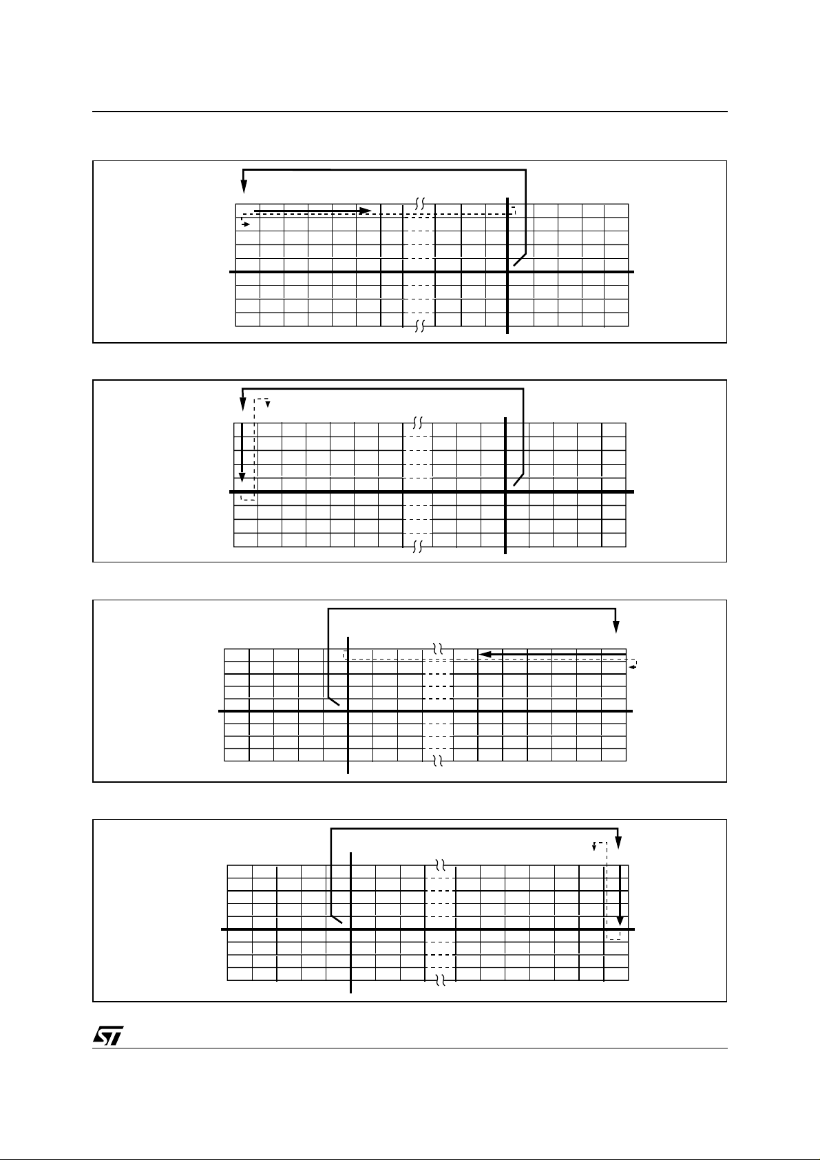
Figure 10. Automatic data RAM writing sequence with X-Y Carriage Return (V=0; MX=0)
STE2002
BANK 0
0123
BANK 1
BANK 2
Y CARR
BANK 11
BANK 12
X CARR
124 125 126 127
Figure 11. Automatic data RAM writing sequence with X-Y Carriage Return (V=1; MX=0)
BANK 0
0123
BANK 1
BANK 2
Y CARR
BANK 11
BANK 12
X CARR
124 125 126 127
Figure 12. Automatic data RAM writing sequence with X-Y Carriage Return (V=0; MX=1)
X CARR
BANK 0
BANK 1
BANK 2
Y CARR
BANK 11
BANK 12
0
123124125126127
Figure 13. Automatic data RAM writing sequence with X-Y Carriage Return (V=1; MX=1)
X CARR
BANK 0
BANK 1
BANK 2
Y CARR
BANK 11
BANK 12
0
123124125126127
11/51
STE2002
Figure 14. Data RA M Byte or ga n iza ti on with D0 = 0
MSB
BANK 0
BANK 1
BANK 2
BANK 3
LSB
BANK 4
BANK 5
BANK 6
BANK 7
BANK 8
BANK 9
BANK 10
BANK 11
BANK 12
Figure 15. Data RA M Byte or ga n iza ti on with D0 = 1
LSB
BANK 0
BANK 1
BANK 2
BANK 3
MSB
BANK 4
BANK 5
BANK 6
BANK 7
BANK 8
BANK 9
BANK 10
BANK 11
BANK 12
0
1 2 3 124 125 126 127
0
1 2 3 124 125 126 127
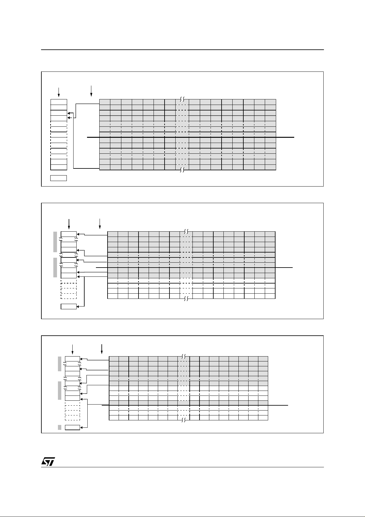
Figure 16. Memory Rows vs. Row drivers mapping with MY=0, MUX81, ICON MODE=0,1
ICON MODE=1 ICON MODE=0
R 0
R 1
R 2
R 3
R 79
R 80
ICON
Figure 17.
ROW DRIVER
ICON MODE=1
R 0
R 1
R 2
R 3
ROW DRIVERROW DRIVER
R 0
R 1
R 2
R 3
R 79
R 80
Memory Row s vs. R ow drivers m apping with MY= 0, MUX 8 1, SCRO LL POIN TER = +3, ICON MODE=1
PHYSICAL MEMORY ROW
ROW 0
ROW 1
ROW 2
ROW 3
PHYSICAL MEMORY ROW
0
ROW 0
ROW 1
ROW 2
1 2 3 124 125 126 127
ROW 3
ROW 79
ROW 80
0
1 2 3 124 125 126 127
Y-CARRIAGE
ICON ROW
12/51
R 76
R 77
R 78
R 79
R 80
ICON
ROW 79
ROW 80
Y-CARRIAGE
ICON ROW
STE2002
Figure 18. Memory Rows vs. Row drivers mapping with MY=0, MUX 81, SCROLL POINTER=+3, ICON MODE=0
ROW DRIVER
ICON MODE=0
R 0
R 1
R 2
R 3
PHYSICAL MEMORY ROW
0
ROW 0
1 2 3 124 125 126 127
ROW 1
ROW 2
ROW 3
Y-CARRIAGE
R 76
R 77
R 78
R 79
R 80
ROW 79
ROW 80
ROW 161
ICON ROW
ICON
Figure 19. Memory Rows vs. Row drivers mapping with MUX 65 Y-CARRIAGE<=8 SCROLL POINTER=0, ICON MODE=1
ROW DRIVER
R 0
R 30
R 31
N.C.
R 40
R 71
PHYSICAL MEMORY ROW
0
ROW 0
ROW 1
ROW 31
ROW 32
ROW 63
ROW 64
1 2 3 124 125 126 127
Y-CARRIAGE
ICON ROWR 72
N.C.
R 79
R 80
ICON
ROW 96
Figure 20. Memory Rows vs. Row drivers mapping with MUX65, Y-CARRIAGE>8, SCROLL POINTER=0, ICON MODE=1
ROW DRIVER
N.C.
N.C.
R 0
R 31
R 32
R 40
R 71
R 72
R 79
R 80
ICON
PHYSICAL MEMORY ROW
0
ROW 0
ROW 31
ROW 32
ROW 63
ROW 75
ROW 76
ROW 96
1 2 3 124 125 126 127
ICON ROW
Y-CARRIAGE
13/51
STE2002
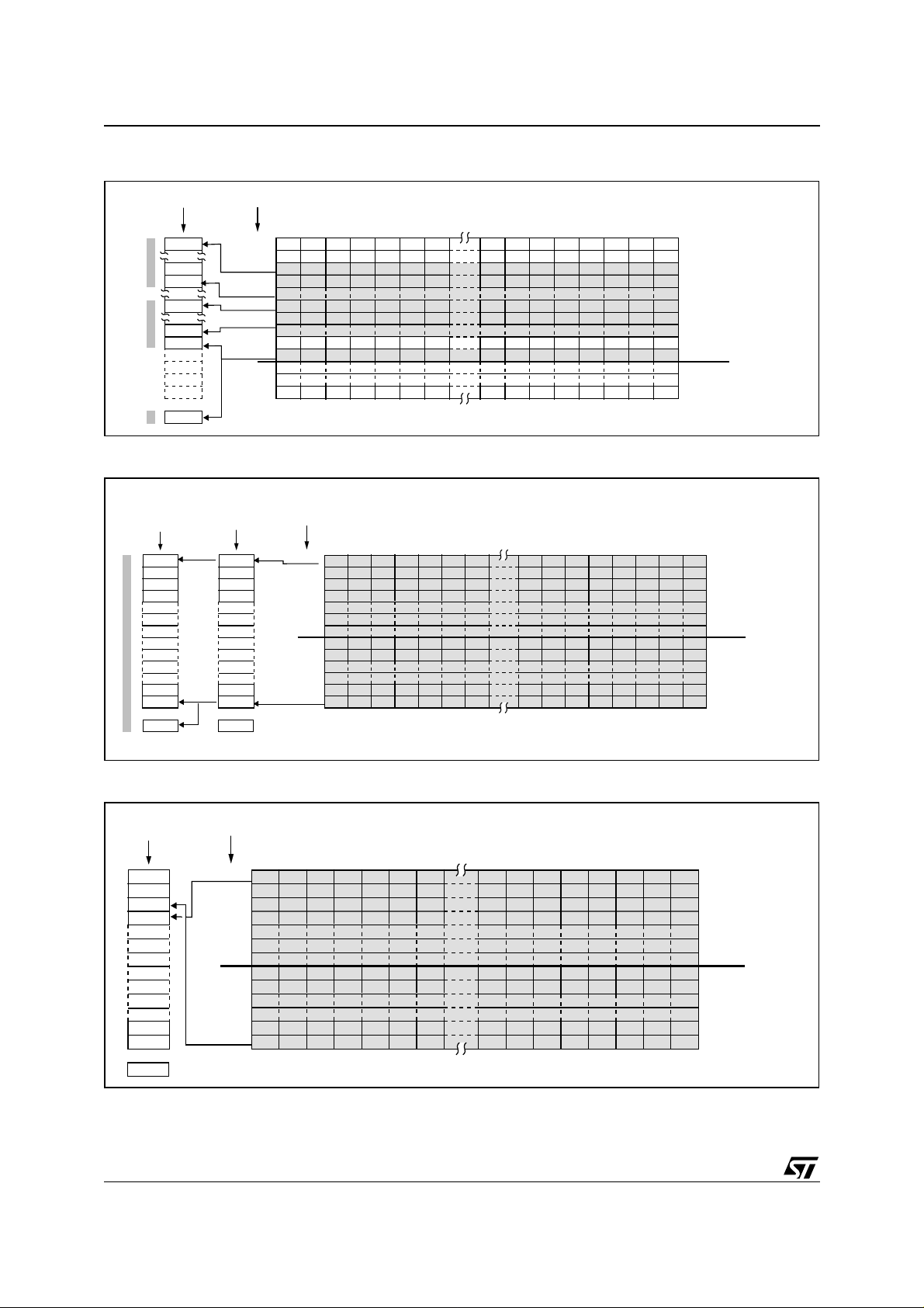
Figure 21. Memory Rows vs. Row drivers mapping with MUX65, Y-CARRIAGE>8, SCROLL POINTER=3, ICON MODE=1,
ROW DRIVER
N.C.
N.C.
R 0
R 30
R 31
R 40
R 71
R 72
R 79
R 80
ICON
PHYSICAL MEMORY ROW
0
ROW 0
ROW 1
ROW 2
ROW 33
ROW 34
ROW 66
ROW 75
ROW 76
ROW 96
1 2 3 124 125 126 127
ICON ROW
Y-CARRIAGE
Figure 22. Memory Rows vs. Row drivers mapping with MY=1, MUX81, ICON MODE 0,1 SCROLL POINTER=0
ROW DRIVER
ICON MODE=1
R 79
R 78
ROW DRIVER
ICON MODE=0
R 80
R 79
PHYSICAL MEMORY ROW
0
ROW 0
ROW 1
ROW 2
ROW 3
1 2 3 124 125 126 127
Y-CARRIAGE
R 2
R 1
R 0
R 80
ICON
R 3
R 2
R 1
R 0
ICON
ROW 79
ROW 80
ICON ROW
Figure 23. Memory Rows vs. Row drivers mapping with MY=1, MUX81, SCROLL OFFSET= +3, ICON MODE =0
ROW DRIVER
ICON MODE=0
R 80
R 78
R 79
R 77
R 76
R 1
R 0
ICON
PHYSICAL MEMORY ROW
0
ROW 0
1 2 3 124 125 126 127
ROW 1
ROW 2
ROW 3
ROW 79
ROW 80
Y-CARRIAGE
ICON ROW
14/51
STE2002
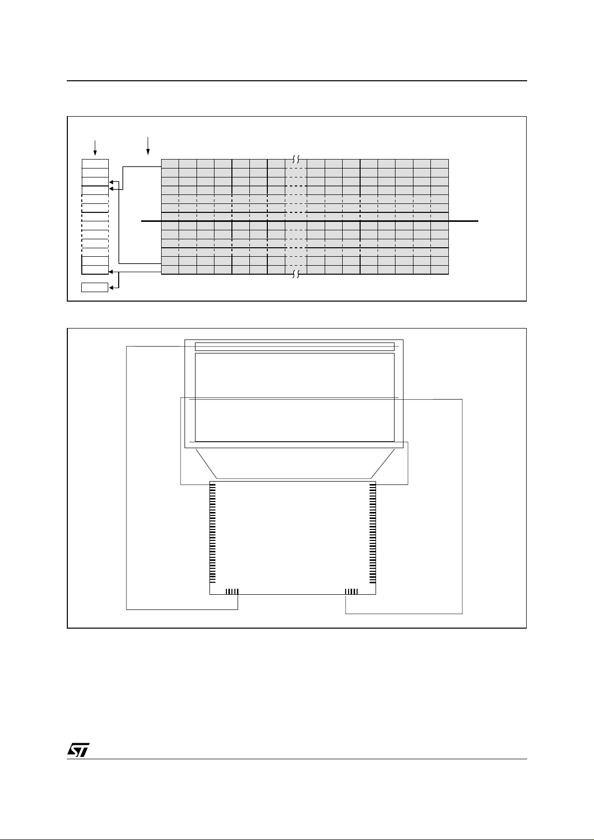
Figure 24. Memory Rows vs. Row drivers mapping with MY=1, MUX81, SCROLL OFFSET= +3, ICON MODE =1
ROW DRIVER
ICON MODE=1
R 79
R 78
R 77
R 76
PHYSICAL MEMORY ROW
0
ROW 0
1 2 3 124 125 126 127
ROW 1
ROW 2
ROW 3
SCROLL OFFSET +3
R 1
R 0
R 80
ROW 79
ROW 80
ICON
Figure 25. Row Drivers vs. LCD Panel Interconnection in MUX81 Mode
ICON
81x128
MUX 81 Mode
Y-CARRIAGE
ICON ROW
ROW DRIVERS
COLUMN DRIVERS
R40
R41
R42
R43
R44
R45
R46
R47
R48
R49
R50
R51
R52
R53
R54
R55
R56
R57
STE2002
R58
R59
R60
R61
R62
R63
R64
R65
R66
R67
R68
R69
R70
R71
R80/ICON
R72
R73
R74
R79
R78
R77
R76
R75
ICON
R 0
R 1
R 2
R 3
R 4
R 5
ROW DRIVERS
R 6
R 7
R 8
R 9
R10
R11
R12
R13
R14
R15
R16
R17
R18
R19
R20
R21
R22
R23
R24
R25
R26
R27
R28
R29
R30
R31
R32
R33
R37
R36
R38
R39
R35
R34
LR0012
15/51
STE2002
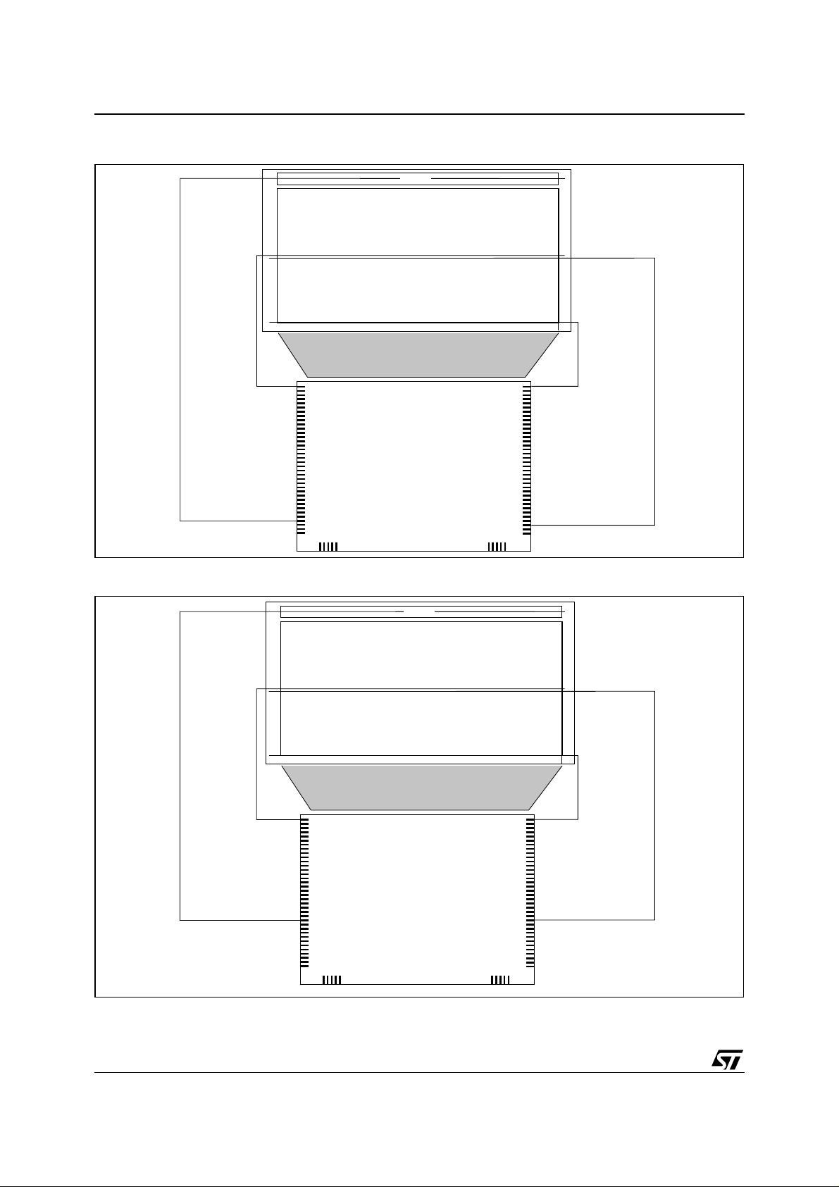
Figure 26. Row Drivers vs. LCD Panel Interconnection in MUX65 Mode
ICON
65x128
MUX 65 Mode
COLUMN DRIVERS
ROW DRIVERS
R40
R41
R42
R43
R44
R45
R46
R47
R48
R49
R50
R51
R52
R53
R54
R55
R56
R57
R58
R59
R60
STE2002
R61
R62
R63
R64
R65
R66
R67
R68
R69
R70
R71
R80/ICON
R72
R73
R74
R79
R78
R77
R76
R75
ICON
R 0
R 1
R 2
R 3
R 4
R 5
R 6
R 7
R 8
R 9
R10
R11
R12
R13
R14
R15
R16
R17
R18
R19
R20
R21
R22
R23
R24
R25
R26
R27
R28
R29
R30
R31
R32
R33
R37
R36
R38
R39
R35
R34
Figure 27. Row Drivers vs. LCD Panel Interconnection in MUX49 Mode
ICON
49x128
MUX 49 Mode
COLUMN DRIVERS
ROW DRIVERS
LR0014
16/51
ROW DRIVERS
R40
R41
R42
R43
R44
R45
R46
R47
R48
R49
R50
R51
R52
R53
R54
R55
R56
R57
R58
R59
R60
STE2002
R61
R62
R63
R64
R65
R66
R67
R68
R69
R70
R71
R80/ICON
R72
R73
R74
R79
R78
R77
R76
R75
ICON
R 0
R 1
R 2
R 3
R 4
R 5
R 6
R 7
R 8
R 9
R10
R11
ROW DRIVERS
R12
R13
R14
R15
R16
R17
R18
R19
R20
R21
R22
R23
R24
R25
R26
R27
R28
R29
R30
R31
LR0013
R32
R33
R37
R36
R38
R39
R35
R34
 Loading...