

STE2002
81 X 128 SINGLE CHIP LCD CONTROLLER / DRIVER
■ 104 x 128 bits Display Data RAM
■ Programmable MUX rate
■ Programmable Frame Rate
■ X,Y Programmable Carriage Return
■ Dual Partial Display Mode
■ Row by Row Scrolling
■ Automatic data RAM Blanking procedure
■ Selectable Input Interface:
2
• I
C Bus Fast and Hs-mode (read and write)
• Parallel Interface (read and write)
• Serial Interface (read and write)
■ Fully Integrated Oscillat or requires no ex ternal
components
■ CMOS Compatible Inputs
■ Fully Integrated Configurable LCD bias voltage
generator with:
• Selectabl e
multiplication factor (up to 6X)
• Effective sensing for High Precision Output
• Eight selectable temperature compensation
coefficients
■ Designed for chip-on-glass (COG) applications
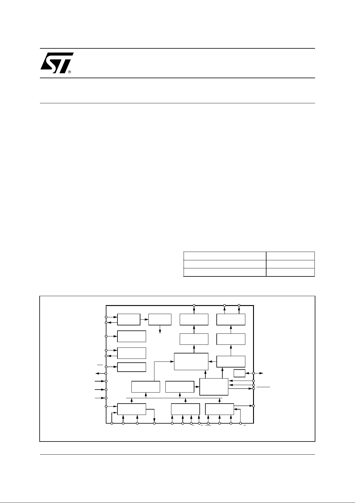
Figure 1. Block Diagram
■ Low Power Consumption, suitable for battery
operated systems
■ Logic Supply Voltage range from 1.7 to 3.6V
■ High Voltage Generator Supply Voltage range
from 1.75 to 4.2V
■ Display Supply Voltage range from 4.5 to 11V
■ Backward Compatibility with STE2001
DESCRIPTION
The STE2002 is a low power CMOS LCD controller
driver. Designed to drive a 81 rows by 128 columns
graphic display, provides all necessary functions in a
single chip, including on-chip LCD supply and bias
voltages generators, resulting in a minimum of externals components and in a very low power consumption. The STE2002 features three standard interfaces
(Seria l, P ar allel & I
host
m
controller.
Bumped Wafers STE2002DIE1
Bumped Dice on Waffle Pack
2
C) for ease of interfacing with the
Type Ordering Number
STE2002DIE2
September 2002
OSC_IN
OSC_OUT
VLCDIN
VLCDSENSE
VLCDOUT
RES
VSSAUX
VDD1,2
V
SS
SEL1,2
SA1
SAO
OSC
BIAS VOLTAGE
GENERATOR
HIGH VOLTAGE
GENERATOR
RESET
REGISTER
I2CBUS
SDA_IN SDA_OUTSCL
DATA
TIMING
GENERATOR
CLOCK
INSTRUCTION
DB0 to DB7 E PD/C
CO to C127 R0 to R80
COLUMN
DRIVERS
DATA
LATCHES
104 x 128
RAM
DISPLAY
REGISTER
PARALLEL SERIAL
CONTROL
LOGIC
SCE SDIN SCLK SD/C
R/W
ROW
DRIVERS
SHIFT
REGISTER
SCROLL
LOGIC
ICON
TEST
TEST_1_14
ICON_MODE
EXT
BSY_FLG
SOUT
1/51
STE2002
PIN DESCRIPTION
N° Pad T ype Function
R0 to R80 129-169
O LCD Row Driver Output
282-322
ICON 323 O ICON Row Driver
C0 to C127 1-128 O LCD Column Driver Output
SS 236-255 GND Ground pads.
V
DD1 188-199 Supply IC Positive Power Supply
V
DD2 200-211 Supply Internal Generator Supply Voltages.
V
LCDIN 261-270 Supply LCD Supply Voltages for the Column and Row Output Drivers.
V
VLCDOUT 273-282 Supply Voltage Multiplier Output
V
LCDSENSE
271-272 Supply Voltage Multiplier Regulation Input. V
Sensing for Output Voltage Fine
LCDOUT
Tuning
V
SSAUX
180, 231,
O Ground Reference for Selection Pins Configuration
218
SEL1,2 184,185 I Interface Mode Selection
EXT 1 83 I Extended Instruction Set Selecti on
EXT PAD CONFIG INSTRUCTION SET SELECTED
VSS or VSSAUX BASIC
VDD1 EXTENDED
ICON_MO
DE
186 I ICON ROW Management
ICON MODE PAD CONFIG ICON MODE STATUS
VSS or VSSAUX DISABLED
VDD1 ENABLED
SDA_IN 234 I
SDA_OUT 232 O
SCL 235 I
SA0 182 I
SA1 181 I
2
C Bus Data In
I
2
C Bus Data Out
I
2
C bus Clock
I
2
C Slave Address BIT 0
I
2
C Slave Address BIT 1
I
OSCIN 187 I External Oscillator Input
OSCOUT 260 O Internal/External Oscillator Out
RES
230 I Reset Input. Active Low.
DB0 to DB7 220-227 I/O Parallel Interface 8 Bit Data Bus
R/W
219 I Parallel Interface Read & Write Control Line
E 229 I Parallel Interface Data Latch Signal.
PD/C
228 I Parallel Interface Data/Command Selector
SDIN 214 I Serial Interface Data Input
2/51
STE2002
PIN DESCRIPTION
N° Pad Type Function
SCLK 217 I Serial Interface Clock
SCE
SD/C
SOUT 213 O Serial Out
BSYFLG
T1 to T14 170-179,
(continued)
216 I Serial Interface ENABLE. When Low the Incoming Data are Clocked In.
215 I Serial Interface Data/Command Selector
212 O Active Procedure Flag. Notice if There is an ongoing Internal Operation or an
active reset. Active Low.
I/O Test Pads. - A 50kohm pull-down resistor is added on input pis.
256-259
Test Num. Pin Configuration
TEST_1
TEST_2
TEST_3
TEST_4
TEST_5
TEST_6
TEST_7
TEST_8
TEST_9
TEST_10
TEST_11
TEST_12
TEST_13
TEST_14
OPEN
VSS / VSSAUX
VSS / VSSAUX
3/51
STE2002
Figure 2. Chip Mechanical Drawing
COL 0
COL 63
COL 64
ROW 0
ICON
MARK_1
STE2002
(0,0)
ROW 34
ROW 35
ROW 39.
MARK_3
MARK_4
VLCDOUT
VLCDSENSE
VLCDIN
OSCOUT
TEST_14
TEST_13
TEST_12
TEST_11
VSS
SCL
SDAIN
SDAOUT
VSSAUX
RES
E
PD/C
D0
D1
D2
D3
D4
D5
D6
D7
R/W
VSSAUX
SCLK
SCE
SD/C
SDIN
SDOUT
BSY_FLG
VDD2
VLCDOUT
VLCDSENSE
VLCDIN
Y
X
VDD2
4/51
COL 127
ROW 40
MARK_2
VDD1
VDD1
OSCIN
ICON_MODE
SEL1
SEL2
EXT_SET
SA0
SA1
VSSAUX
TEST_10
TEST_9
TEST_8
TEST_7
TEST_6
TEST_5
TEST_4
TEST_3
TEST_2
TEST_1
ROW 80/ICON
ROW 79
ROW 76
ROW 75
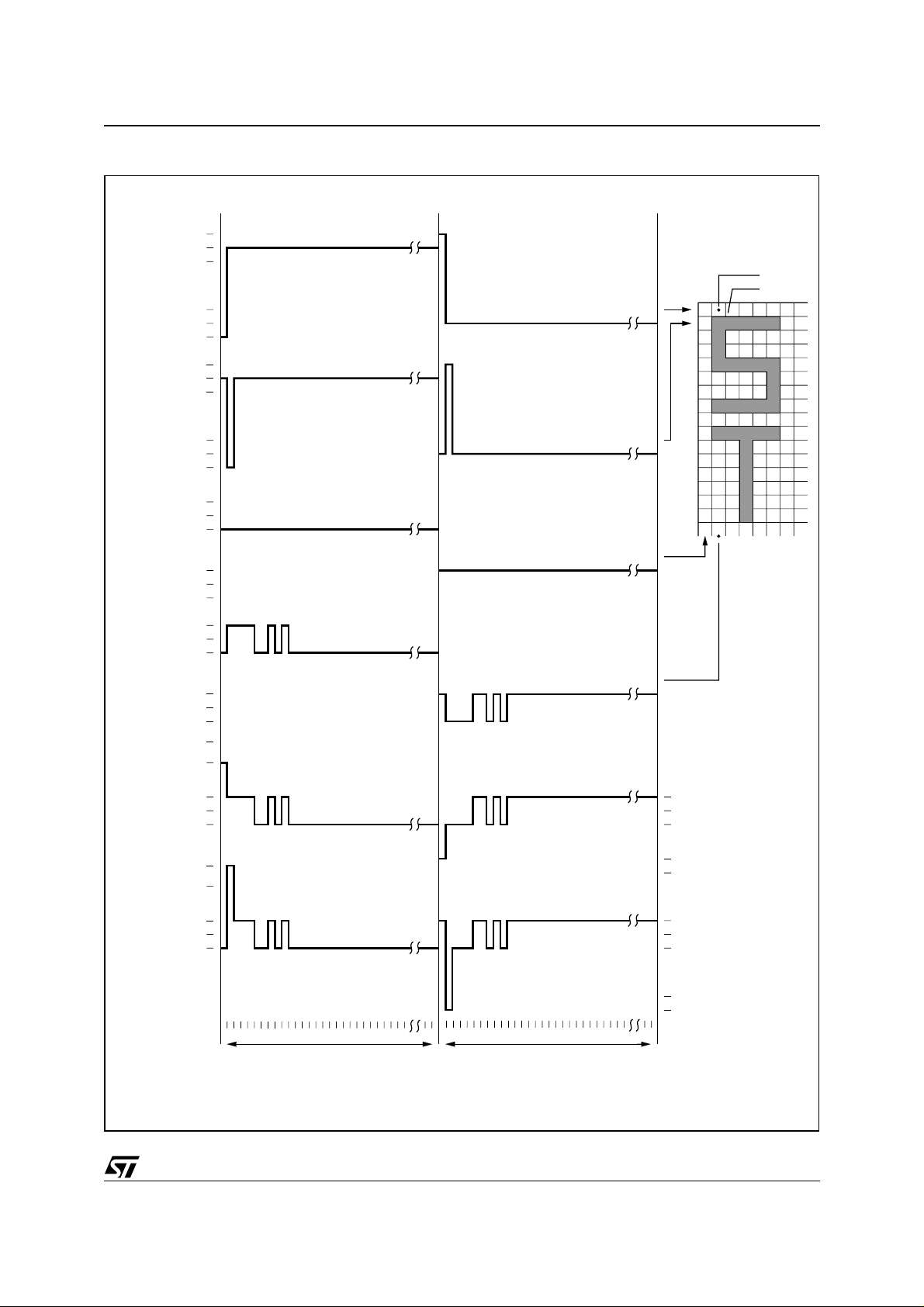
Figure 3. Improved ALTH & PLESKO Driving Method
V
LCD
V
2
V
3
ROW 0
R0 (t)
V
4
V
5
V
SS
V
LCD
V
2
V
3
ROW 1
R1 (t)
V
4
V
5
V
SS
V
LCD
V
2
V
3
COL 0
C0 (t)
V
4
V
5
V
SS
V
LCD
V
2
V
3
COL 1
C1 (t)
V
4
V
5
V
SS
V
- V
LCD
SS
V3 - V
SS
STE2002
∆V1(t)
∆V
(t)
2
V
V
state1
state2
- V
V
LCD
(t)
V3 - V
V
- V
LCD
V3 - V
- V
V
LCD
(t)
V3 - V
(t) = C1(t) - R0(t)
∆V
1
∆V
(t) = C1(t) - R1(t)
2
2
0V
SS
SS
SS
2
0V
SS
0 1 2 3 4 5 6 7 8 9 64
.......
FRAME n FRAME n + 1
0 1 2 3 4 5 6 7 8 9 64
.....
.......
.....
V
4 - V5
0V
V
SS - V5
V4 - V
VSS - V
V
4 - V5
0V
V
SS - V5
V4 - V
VSS - V
D00IN1154
LCD
LCD
LCD
LCD
5/51
STE2002
0
CIRCUIT DESCRIPTION
Supplies Voltages and Gro un ds
is supply voltages to the internal voltage generator (see below). If the internal voltage generator is
V
DD2
not used, this should be c onnected to V
could be different form V
DD2
.
Internal Supply Voltage Ge nerator
The IC has a fully integrated (no external capacitors required) charge pump for the Liquid Crystal Display
supply voltage generation. The multiplying factor can be programmed to be: Auto, X6, X5, X4, X3, X2, using the ’set CP Multiplication’ Command. If Auto is set, the multiplying factor is automatically selected to
have the lowest current consumption in every condition. This make possible to have an input voltage that
changes over time and a constant V
the V
LCDSENSE
pad. For this voltage, eight different temperature coefficients (TC, rate of change with tem-
LCD
perature) can be programmed using th e bits TC1 and TC0 and T2,T1 & T0. This will ensure no cont rast
degradation over the LCD operating range. Using the internal charge pump, the V
must be connected together. An external supply could be connected to V
using the internal generator. In such event the V
the internal voltage generator must be programmed to zero (PRS = [0;0], Vop = 0 - Reset condition).
Oscillator
A fully integrated oscillator (requires no externa l com ponen ts) is presen t to provi de t he clock f or t he Display System. When u sed the O SC pad must be connec ted to V
used and fed into the OSC pin. An oscillator out is provided on the OSCOUT Pad to cascade two or more
drivers
Bias Levels
To properly drive the LCD, six (Including VLCD and VSS) different voltage (Bias ) levels are generated.
The ratios among these levels and VLCD, s hould be selected acc ording to the MUX ratio (m). They are
established to be (Fig. 4):
DD1
pad. V
supplies the rest of the IC. V
DD1
voltage. The output voltage (V
LDCOUT
and V
LCDSENSE
DD1
supply voltage
DD1
LCDOUT
) is tightly controlled through
and V
LCDIN
to supply the LCD without
LCDIN
LCDOUT
pads
must be connected to GND and
pad. An external oscillator could be
LCD
n3+
,
------------ - V
n4+
LCD
n2+
,
------------ - V
n4+
LCD
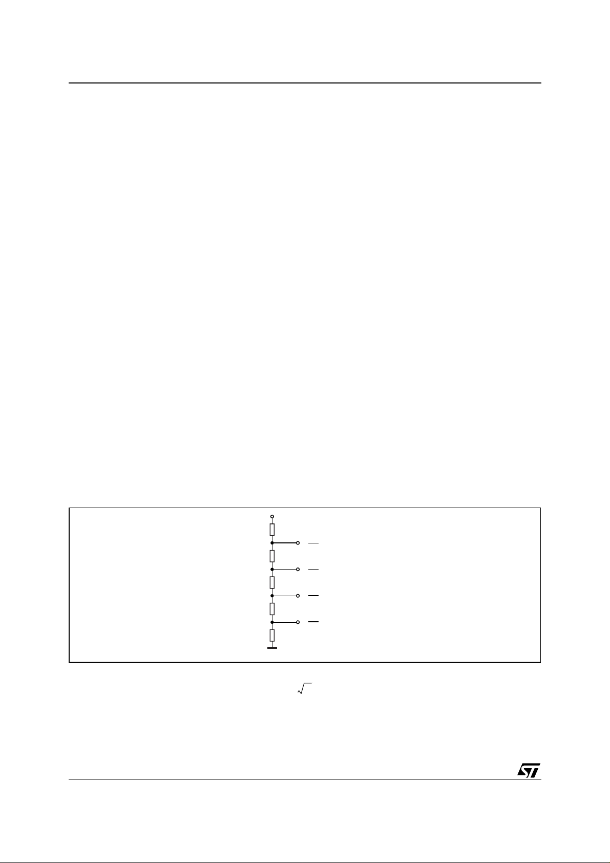
Figure 4. Bias level Generator
R
R
nR
R
R
thus providing an 1/(n+4) ratio, with n calculated from:
nm3–=
For m = 81, n = 6 and an 1/10 ratio is set.
For m = 65, n =5 and an 1/9 ratio is set.
2
,
------------ - V
n4+
V
LCD
n + 3
·V
LCD
n + 4
n + 2
·V
LCD
n + 4
2
·V
LCD
n + 4
1
·V
LCD
n + 4
V
SS
D00IN115
LCD
1
,
------------ - V
n4+
LCD,VSS
6/51

STE2002
The STE2002 provides three bits (BS0, BS1, BS2) for programming the desired Bias Ratio as shown below:
BS2 BS1 BS0 n
0007
0016
0105
0114
1003
1012
1101
1110
The following table Bias Level for m = 65 and m = 81 are provided:
Symbol m = 65 (1/9) m = 81 (1/10)
V1 V
V2 8/9*V
V3 7/9*V
V4 2/9*V V
V5 1/9 *V
V6 V
LCD
SS
LCD
LCD
LCD
LCD
V
LCD
9/10*V
8/10*V
2/10*V
1/10*V
V
SS
LCD
LCD
LCD
LCD
LCD Voltage Generation
The LCD Voltage at reference temperature (To = 27°C) can be set using the VOP register content according to
the following formula:
V
LCD
(T=To) = V
o = (Ai+VOP · B) (i=0,1,2)
LCD
with the following values:
Symbol Value Unit Note
Ao 2.95 V PRS = [0;0]
A1 6.83 V PRS = [0;1]
A2 10.71 V PRS = [1;0]
B 0.03 03 V
To 27 °C
Note that the three PRS values produce three adjacent ranges for VLCD. If the V
register and PRS bits are
OP
set to zero the internal voltage generator is switched off.
The proper value for the VLCD is a function of the Liquid Crystal Threshold Voltage (Vth) and of the Multiplexing
Rate. A general expression for this is:
1m+
----------------------------------- - V
V
LCD(to)
op
-----------------------------------------=
V
⋅=
th
1
⋅
21
-------- -–
m
= 6.85 · V
th
6.85 VthAi–⋅()
0.03
For MUX Rate m = 65 the ideal V
than:
LCD
is:
V
LCD
7/51

STE2002
Temperature Coefficient
As the viscosity, and therefore the contrast, of the LCD are subject to change with temperature, there's the need
to vary the LCD Voltage with temperature. The STE2002 provides the possibility to change the VLCD in a linear
fashion against temperature with eight different Temperature Coefficient selectable through the T2, T1 and T0
bits. Only four of them are available with basic instruction set (TC1 & TC0 Bits).
NAME TC1 TC0 Value Unit
TC0 0 0
TC2 0 1
TC3 1 0
TC6 1 1
-0.7 · 10
-1.05· 10
-2.1 · 10
-0.0· 10
-3
-3
-3
-3
NAME TC2 TC1 TC0 Value Unit
TC0 0 0 0
TC1 0 1 1
TC2 1 0 0
TC3 1 1 1
TC4 1 1 1
TC5 1 1 1
TC6 1 1 1
TC7 1 1 1
-0.35 · 10
-0.7 · 10
-1.05· 10
-1.4 · 10
-1.75· 10
-2.1 · 10
-0.0· 10
-2.3· 10
-3
-3
-3
-3
-3
-3
-3
-3
Figure 5.
1/ °C
1/°C
1/°C
1/°C
1/ °C
1/°C
1/°C
1/°C
1/°C
1/°C
1/°C
1/°C
LCD
V
0
A
00h 01h 02h 03h 04h 05h ….
Finally, the V
8/51
B
1
0
A
+ B
7Ch 7Dh 7Eh
PRS = [0;0]
voltage at a given (T) temperature can be calculated as:
LCD
A
7Fh 00h 01h 02h
(T) = V
V
LCD
03h 04h
05h …. 7Ch
PRS = [0;1]
o · [1 + (T-To) · T C]
LCD
7Dh 7Eh 7Fh
2
A
00h 01h 02h 03h 04h
05h 7Ch
….
PRS = [1;0]
7Dh 7Eh 7Fh
O
V

STE2002
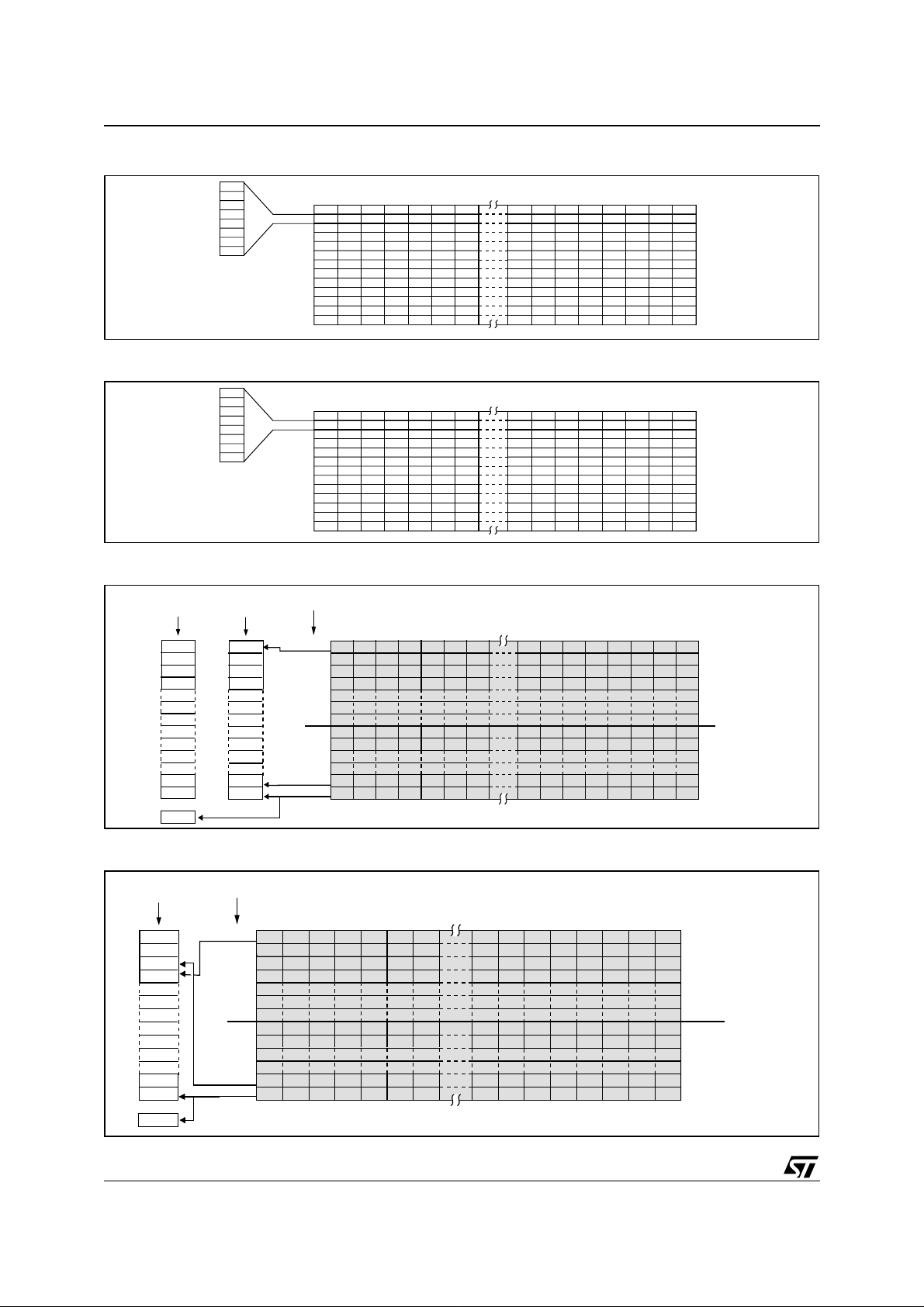
Display Data RAM
The STE2002, provides an 104X128 bits Static RAM to store Display da ta. This is organized into 13
(Bank0 to Bank12) banks with 128 Bytes. One of these banks (128 bits wide) can be used for Icons. RAM
access is accomplished in either one of the Bus Interfaces provided (s ee bel ow). Allowed address es are
X0 to X127 (Horizontal) and Y0 to Y12 (Vertical).
When writing to RAM, four addressing mode are provided:
• Normal Horizontal (MX=0 and V=0), having the column with address X= 0 located on the left of the memory map. The X pointer is increased after each byte written. After the last column address (X=X-Carriage), Y address pointer is set to jump to the following bank and X restarts from X=0. (Fig. 6)
• Normal Vertical (MX=0 and V=1), having the column with address X= 0 located on the left of the memory
map. The Y pointer is increased after each byte written. After th e l ast Y bank address (Y =Y-Carriage ),
X address pointer is set to jump to next column and Y restarts from Y=0 (Fig. 7).
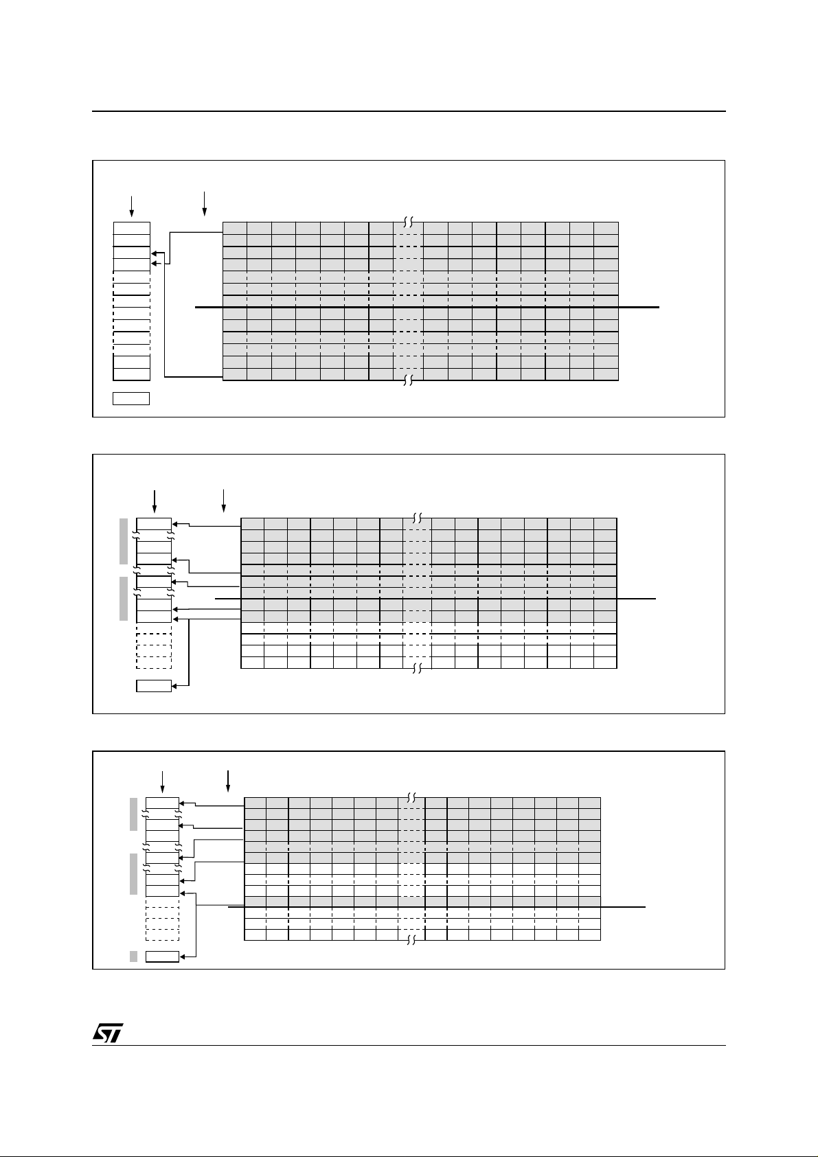
• Mirrored Horizontal (MX=1 and V=0), having the column with address X= 0 located on the right of the
memory map. The X pointer is increased af ter each byte written. After the last column address (X=XCarriage), Y address pointer is set to jump to the next bank and X restarts from X=0 (fig. 8).
• Mirrored Vertical (MX=1 and V=1), having the column with address X= 0 located on the right of the memory map. The Y pointer is increased after each byte written. After the last Y bank address (Y=Y-Carriage), the X pointer is set to jump to next column and Y restarts from Y=0 (fig. 9).
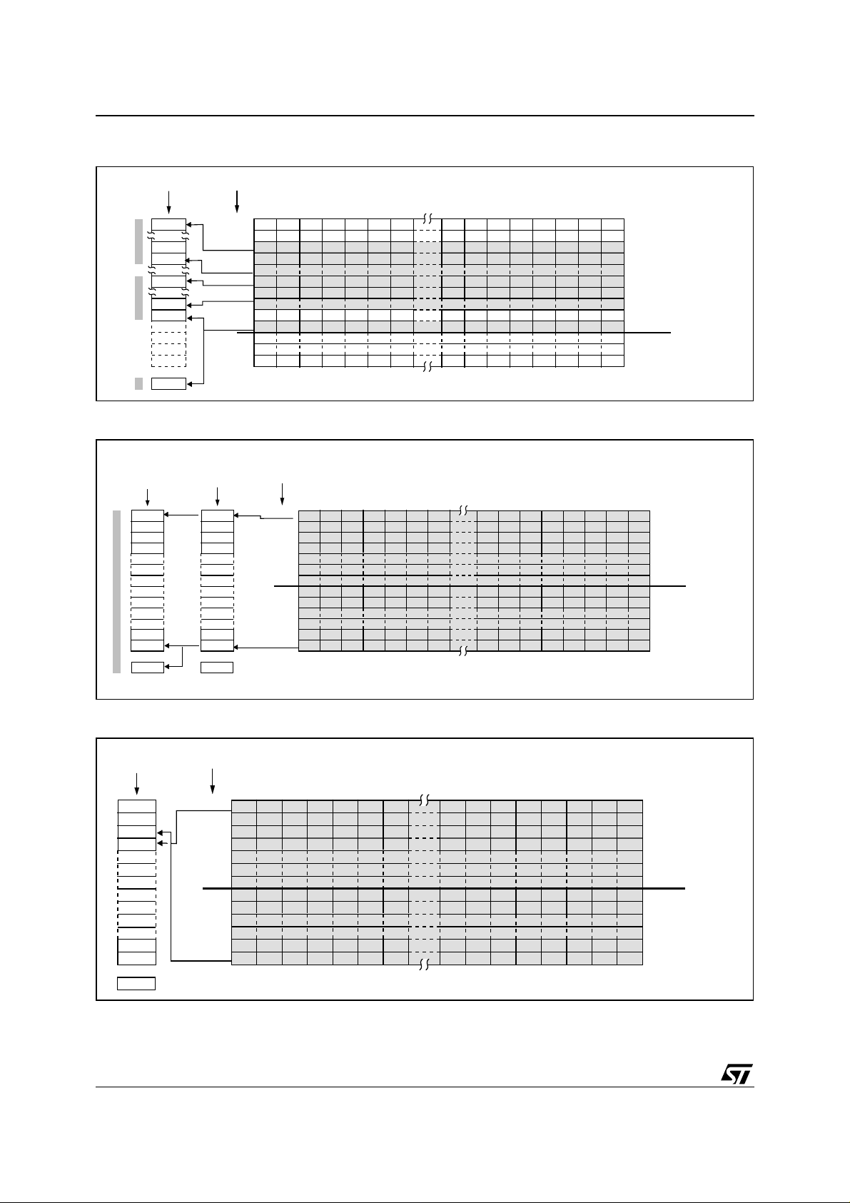
After the last allowed address (X;Y)=(X-Carriage; Y-Carriage), the address pointers always jump to the
cell with address (X;Y) = (0;0) (Fi. 10, 11, 12 & 13).
Data bytes in the memory could have the MSB either on top (D0 = 0, Fig.14) or on the bottom (D0=1, Fig.
15).
The STE2002 provides also means to alter the normal output addressing. A mirroring of the Display along
the X axis is enabled setting t o a l ogic one MY bit.This function does n't af fect t he cont ent of the me mory
RAM. It is only related to the visualization process.
When ICON MODE=1 the Icon Row is not mirrored with MY and is not scrolled. When ICON Mode=0 the
Icon Row is like the other graphic lines and is mirrored and scrolled.
Four are the multiplex ratio avai lable when the partial d isplay mode is disabled (MUX 33 , MUX 49, MUX
65 and MUX 81).
Only a subset of writable rows are output on Row drivers.
When Y-Carriage<MUX/8, if Mux 65 is selected only the first 65 m emory r ows are v isualized, if Mux 49 i s
selected only the first 49 memory rows are visualized, if Mux 33 is selected only the first 33 memory rows
are visualized. All unused Row and Column drivers must be left floating.
When Y-Carriage<MUX/8, the icon Bank i s located t o B A NK 10 in MUX 81 Mode, to BANK8 i n M U X 65
Mode, to BANK 6 in MUX 49 Mode and to BANK 4 in MUX 33 Mode.
When Y-Carriage>MUX/8 lines only 33, 49, 65 or 81 lines are visualized but it is possible to select which
lines of DDRAM are connected on the output drivers. The DDRAM rows to visualized can be sel ected in
the 0-Y-Carriage*8 range using the scrolling function.
When Y-Carriage>MUX lines, the icon row is moved in DDRAM to the first row of the Y-CARRIAGE Return BANK even if it is always connected on the same output Driver.
When MY=0, the icon Row is output on R80 in mux 81 mode, on R72 in MUX 65, on R64 in MUX49 and
on R56 in MUX 33.
When MY=1, and ICON MODE=1, the icon Row is output on R80 in mux 81 mode, on R72 in MUX 65, on
R64 in MUX49 and on R56 in MUX 33.
When MY=1, and ICON MODE=0, the icon Row is output on R0 whatever is the MUX Rate.
When ICON MODE =1, the Memory ICON Row content is output on ICON Pad.
If Not Used ICON Pad must be left floating.
9/51
STE2002
Figure 6. Auto m at ic da ta RAM wri t in g sequence with V=0 and Data RAM N or m a l Form a t ( MX= 0 )1
BANK 0
BANK 1
BANK 2
BANK 3
BANK 4
BANK 5
BANK 6
BANK 7
BANK 8
BANK 9
BANK 10
BANK 11
BANK 12
0123 124125126127
Figure 7. Auto m at ic da ta RAM wri t in g sequence with V=1 and Data RAM N or m a l Form a t ( MX= 0 )
BANK 0
BANK 1
BANK 2
BANK 3
BANK 4
BANK 5
BANK 6
BANK 7
BANK 8
BANK 9
BANK 10
BANK 11
BANK 12
0123 124125126127
Figure 8. Automatic data RAM writing sequence with V=0 and Data RAM Mirrored Format (MX=1)
1
1
127 126 125 124 3 2 1 0
BANK 0
BANK 1
BANK 2
BANK 3
BANK 4
BANK 5
BANK 6
BANK 7
BANK 8
BANK 9
BANK 10
BANK 11
BANK 12
Figure 9. Automatic data RAM writing sequence with V=1 and Data RAM Mirrored Format (MX=1)1
BANK 0
BANK 1
BANK 2
BANK 3
BANK 4
BANK 5
BANK 6
BANK 7
BANK 8
BANK 9
BANK 10
BANK 11
BANK 12
1. X Carriage=127; Y-Carriage = 12
127 126 125 124 3 2 1 0
10/51
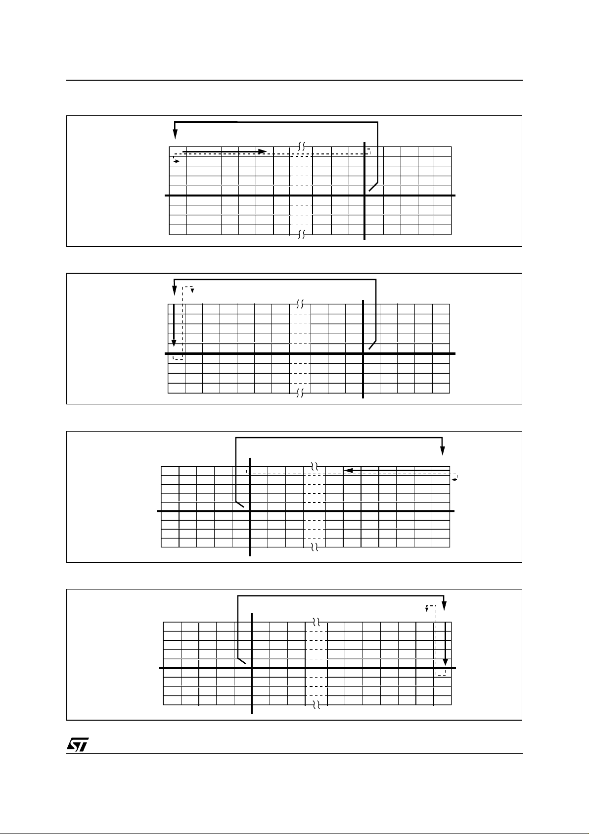
Figure 10. Automatic data RAM writing sequence with X-Y Carriage Return (V=0; MX=0)
STE2002
BANK 0
0123
BANK 1
BANK 2
Y CARR
BANK 11
BANK 12
X CARR
124 125 126 127
Figure 11. Automatic data RAM writing sequence with X-Y Carriage Return (V=1; MX=0)
BANK 0
0123
BANK 1
BANK 2
Y CARR
BANK 11
BANK 12
X CARR
124 125 126 127
Figure 12. Automatic data RAM writing sequence with X-Y Carriage Return (V=0; MX=1)
X CARR
BANK 0
BANK 1
BANK 2
Y CARR
BANK 11
BANK 12
0
123124125126127
Figure 13. Automatic data RAM writing sequence with X-Y Carriage Return (V=1; MX=1)
X CARR
BANK 0
BANK 1
BANK 2
Y CARR
BANK 11
BANK 12
0
123124125126127
11/51
STE2002
Figure 14. Data RA M Byte or ga n iza ti on with D0 = 0
MSB
BANK 0
BANK 1
BANK 2
BANK 3
LSB
BANK 4
BANK 5
BANK 6
BANK 7
BANK 8
BANK 9
BANK 10
BANK 11
BANK 12
Figure 15. Data RA M Byte or ga n iza ti on with D0 = 1
LSB
BANK 0
BANK 1
BANK 2
BANK 3
MSB
BANK 4
BANK 5
BANK 6
BANK 7
BANK 8
BANK 9
BANK 10
BANK 11
BANK 12
0
1 2 3 124 125 126 127
0
1 2 3 124 125 126 127
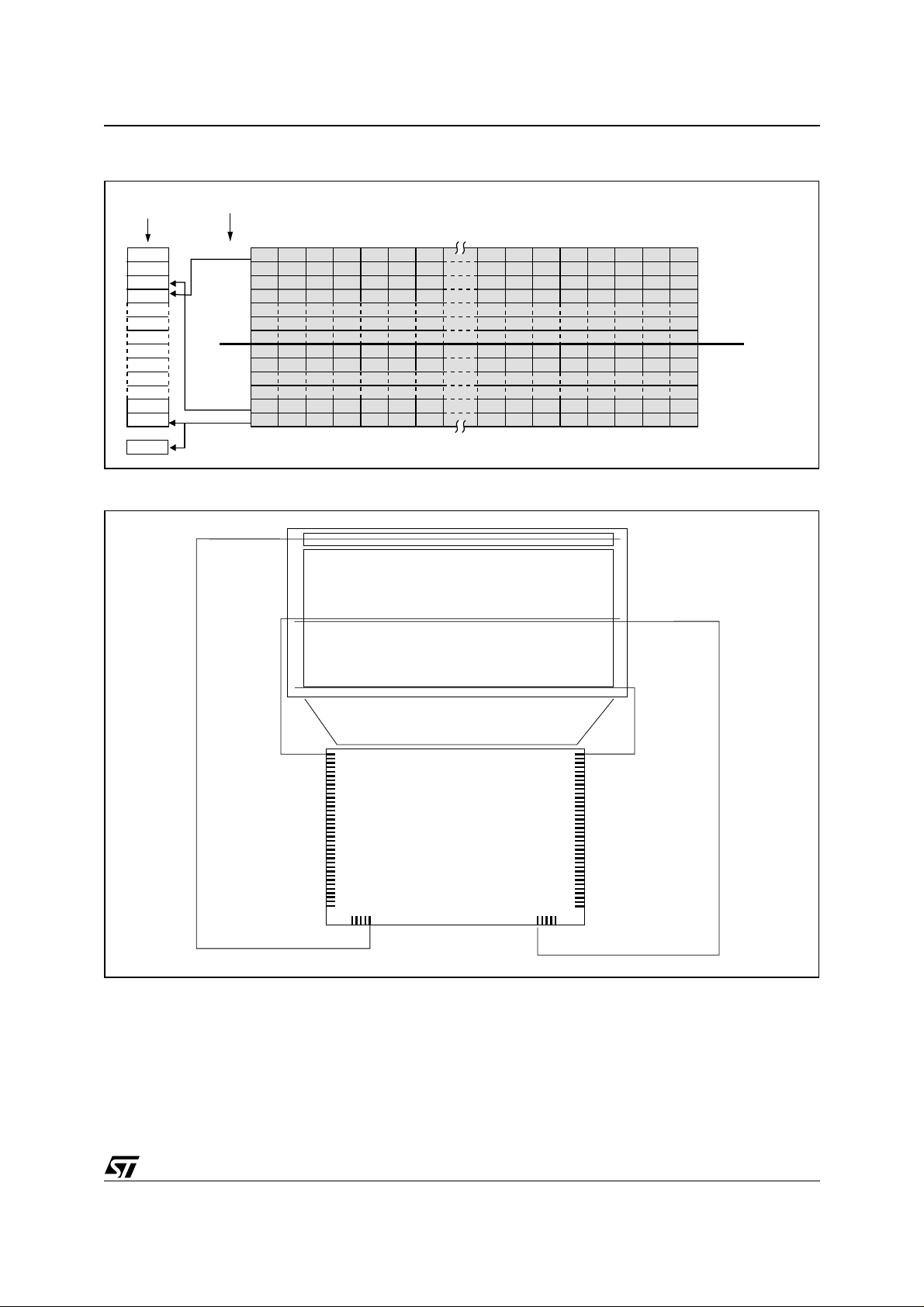
Figure 16. Memory Rows vs. Row drivers mapping with MY=0, MUX81, ICON MODE=0,1
ICON MODE=1 ICON MODE=0
R 0
R 1
R 2
R 3
R 79
R 80
ICON
Figure 17.
ROW DRIVER
ICON MODE=1
R 0
R 1
R 2
R 3
ROW DRIVERROW DRIVER
R 0
R 1
R 2
R 3
R 79
R 80
Memory Row s vs. R ow drivers m apping with MY= 0, MUX 8 1, SCRO LL POIN TER = +3, ICON MODE=1
PHYSICAL MEMORY ROW
ROW 0
ROW 1
ROW 2
ROW 3
PHYSICAL MEMORY ROW
0
ROW 0
ROW 1
ROW 2
1 2 3 124 125 126 127
ROW 3
ROW 79
ROW 80
0
1 2 3 124 125 126 127
Y-CARRIAGE
ICON ROW
12/51
R 76
R 77
R 78
R 79
R 80
ICON
ROW 79
ROW 80
Y-CARRIAGE
ICON ROW
STE2002
Figure 18. Memory Rows vs. Row drivers mapping with MY=0, MUX 81, SCROLL POINTER=+3, ICON MODE=0
ROW DRIVER
ICON MODE=0
R 0
R 1
R 2
R 3
PHYSICAL MEMORY ROW
0
ROW 0
1 2 3 124 125 126 127
ROW 1
ROW 2
ROW 3
Y-CARRIAGE
R 76
R 77
R 78
R 79
R 80
ROW 79
ROW 80
ROW 161
ICON ROW
ICON
Figure 19. Memory Rows vs. Row drivers mapping with MUX 65 Y-CARRIAGE<=8 SCROLL POINTER=0, ICON MODE=1
ROW DRIVER
R 0
R 30
R 31
N.C.
R 40
R 71
PHYSICAL MEMORY ROW
0
ROW 0
ROW 1
ROW 31
ROW 32
ROW 63
ROW 64
1 2 3 124 125 126 127
Y-CARRIAGE
ICON ROWR 72
N.C.
R 79
R 80
ICON
ROW 96
Figure 20. Memory Rows vs. Row drivers mapping with MUX65, Y-CARRIAGE>8, SCROLL POINTER=0, ICON MODE=1
ROW DRIVER
N.C.
N.C.
R 0
R 31
R 32
R 40
R 71
R 72
R 79
R 80
ICON
PHYSICAL MEMORY ROW
0
ROW 0
ROW 31
ROW 32
ROW 63
ROW 75
ROW 76
ROW 96
1 2 3 124 125 126 127
ICON ROW
Y-CARRIAGE
13/51
STE2002
Figure 21. Memory Rows vs. Row drivers mapping with MUX65, Y-CARRIAGE>8, SCROLL POINTER=3, ICON MODE=1,
ROW DRIVER
N.C.
N.C.
R 0
R 30
R 31
R 40
R 71
R 72
R 79
R 80
ICON
PHYSICAL MEMORY ROW
0
ROW 0
ROW 1
ROW 2
ROW 33
ROW 34
ROW 66
ROW 75
ROW 76
ROW 96
1 2 3 124 125 126 127
ICON ROW
Y-CARRIAGE
Figure 22. Memory Rows vs. Row drivers mapping with MY=1, MUX81, ICON MODE 0,1 SCROLL POINTER=0
ROW DRIVER
ICON MODE=1
R 79
R 78
ROW DRIVER
ICON MODE=0
R 80
R 79
PHYSICAL MEMORY ROW
0
ROW 0
ROW 1
ROW 2
ROW 3
1 2 3 124 125 126 127
Y-CARRIAGE
R 2
R 1
R 0
R 80
ICON
R 3
R 2
R 1
R 0
ICON
ROW 79
ROW 80
ICON ROW
Figure 23. Memory Rows vs. Row drivers mapping with MY=1, MUX81, SCROLL OFFSET= +3, ICON MODE =0
ROW DRIVER
ICON MODE=0
R 80
R 78
R 79
R 77
R 76
R 1
R 0
ICON
PHYSICAL MEMORY ROW
0
ROW 0
1 2 3 124 125 126 127
ROW 1
ROW 2
ROW 3
ROW 79
ROW 80
Y-CARRIAGE
ICON ROW
14/51
STE2002
Figure 24. Memory Rows vs. Row drivers mapping with MY=1, MUX81, SCROLL OFFSET= +3, ICON MODE =1
ROW DRIVER
ICON MODE=1
R 79
R 78
R 77
R 76
PHYSICAL MEMORY ROW
0
ROW 0
1 2 3 124 125 126 127
ROW 1
ROW 2
ROW 3
SCROLL OFFSET +3
R 1
R 0
R 80
ROW 79
ROW 80
ICON
Figure 25. Row Drivers vs. LCD Panel Interconnection in MUX81 Mode
ICON
81x128
MUX 81 Mode
Y-CARRIAGE
ICON ROW
ROW DRIVERS
COLUMN DRIVERS
R40
R41
R42
R43
R44
R45
R46
R47
R48
R49
R50
R51
R52
R53
R54
R55
R56
R57
STE2002
R58
R59
R60
R61
R62
R63
R64
R65
R66
R67
R68
R69
R70
R71
R80/ICON
R72
R73
R74
R79
R78
R77
R76
R75
ICON
R 0
R 1
R 2
R 3
R 4
R 5
ROW DRIVERS
R 6
R 7
R 8
R 9
R10
R11
R12
R13
R14
R15
R16
R17
R18
R19
R20
R21
R22
R23
R24
R25
R26
R27
R28
R29
R30
R31
R32
R33
R37
R36
R38
R39
R35
R34
LR0012
15/51
STE2002
Figure 26. Row Drivers vs. LCD Panel Interconnection in MUX65 Mode
ICON
65x128
MUX 65 Mode
COLUMN DRIVERS
ROW DRIVERS
R40
R41
R42
R43
R44
R45
R46
R47
R48
R49
R50
R51
R52
R53
R54
R55
R56
R57
R58
R59
R60
STE2002
R61
R62
R63
R64
R65
R66
R67
R68
R69
R70
R71
R80/ICON
R72
R73
R74
R79
R78
R77
R76
R75
ICON
R 0
R 1
R 2
R 3
R 4
R 5
R 6
R 7
R 8
R 9
R10
R11
R12
R13
R14
R15
R16
R17
R18
R19
R20
R21
R22
R23
R24
R25
R26
R27
R28
R29
R30
R31
R32
R33
R37
R36
R38
R39
R35
R34
Figure 27. Row Drivers vs. LCD Panel Interconnection in MUX49 Mode
ICON
49x128
MUX 49 Mode
COLUMN DRIVERS
ROW DRIVERS
LR0014
16/51
ROW DRIVERS
R40
R41
R42
R43
R44
R45
R46
R47
R48
R49
R50
R51
R52
R53
R54
R55
R56
R57
R58
R59
R60
STE2002
R61
R62
R63
R64
R65
R66
R67
R68
R69
R70
R71
R80/ICON
R72
R73
R74
R79
R78
R77
R76
R75
ICON
R 0
R 1
R 2
R 3
R 4
R 5
R 6
R 7
R 8
R 9
R10
R11
ROW DRIVERS
R12
R13
R14
R15
R16
R17
R18
R19
R20
R21
R22
R23
R24
R25
R26
R27
R28
R29
R30
R31
LR0013
R32
R33
R37
R36
R38
R39
R35
R34

Figure 28. Row Drivers vs. LCD Panel Interconnection in MUX33 Mode
ICON
33x128
MUX 33Mode
COLUMN DRIVERS
STE2002
I
nstruction Set
ROW DRIVERS
R40
R41
R42
R43
R44
R45
R46
R47
R48
R49
R50
R51
R52
R53
R54
R55
R56
R57
R58
R59
R60
STE2002
R61
R62
R63
R64
R65
R66
R67
R68
R69
R70
R71
R80/ICON
R72
R73
R74
R79
R78
R77
R76
R75
ICON
R 0
R 1
R 2
R 3
R 4
R 5
ROW DRIVERS
R 6
R 7
R 8
R 9
R10
R11
R12
R13
R14
R15
R16
R17
R18
R19
R20
R21
R22
R23
R24
R25
R26
R27
R28
R29
R30
R31
LR0106
R32
R33
R37
R36
R38
R39
R35
R34
Two different instructions formats are provided:
- With D/C
set to LOW
commands are sent to the Control circuitry.
- With D/C
set to HIGH
the Data RAM is addressed.
Two different instruction set are embedded: the STE2001-like instruction set and the extended instruction
set. To select the STE2001-like instruction set the EXT pad has to be connected to a logic LOW (connect
to VSS). To se lect the extended instruction the EXT pad has to be connected to a logic HIGH (connect to
VDD1).
The instructions have the syntax summarized in Table 1 (basic-set) and Table 2 (extended set)
Reset (RES
)
At power-on, all internal registers are c onfigured with t he defa ult value. T he RAM content is not def ined.
A Reset pulse on RES pad (active low) re-initialize the internal registers content (see Tables 3,4,5,&6).
Applying a reset pulse, every on-going communication with the host controller is interrupted. After the
power-on, the Software Reset instruction can be used to re-load the reset configuration into the internal
registers
The Default configurations is: .
- Horizontal addressing (V = 0)
- Normal instruction set (H[1:0] = 0)
- Normal display (MX = MY = 0)
- Display blank (E = D = 0)
- Address counter X[6: 0] = 0 and Y[4: 0] = 0
- Temperature coefficient (TC[1: 0] = 0)
- Bias system (BS[2: 0] = 0)
- Multiplexing Ratio (M[1:0]=0)
- Frame Rate (FR[1:0]=”75Hz”)
- Power Down (PD = 1)
- Dual Partial Display Disabled (PE=0)
=0
- V
OP
A MEMORY BLANK instruction can be executed to clear the RAM content.
17/51

STE2002
Power Down (PD = 1)
When at Power Down, all LCD outputs are kept at V
are OFF (V
LCDOUT
output is discharged to VSS, and then is possible to disconnect V
Oscillator is in off state. An external clock can be provided. The RAM contents is not cleared.
Memory Blanking Procedure
This instruction allows to fill the memory with "blank" patterns, in order to delete patterns randomly gener-
ated in memory when starting up the device. This in struction substitutes (128X13) single "write" instructions. It is possible to program "Memory Blanking Procedure" only under the following conditions:
- PD bit = 0
The end of the procedure will be notified on the BSY_FLG
running). Any instruction programmed wi th BSY_FLG
programmed for a period equivalent to 128X13 internal write cycles (128X13X1/fclock). The start of Memory blanking procedure will be between one and two fclock cycles from the last active edge (E ri sing edge
for the parallel interface, last SCLK rising edge for the Seria l interface, last SCL rising edge for the I
interface).
Checker Board Procedure
This instruction allows to fill the memory with "checker-board" pattern. It is mainly intended to developers, who
can now simply obtain complex m odule test configuration by means of a single instruction. It is possible to program "Checker Board Procedure" only under the following conditions:
- PD bit = 0
The end of the procedure will be notified on the BSY_FLG
Any instruction programmed with BSY_FLG
LOW will be ignored, that is, no instruction can be programmed for
a period equivalent to 128X13 internal write cycles (128X13X1/fclock). The start of Memory blanking procedure
will be between one and two fclock cycles from the last active edge (E rising edge for the parallel interface, last
SCLK rising edge for the Serial interface, last SCL rising edge for the I
(display off). Bias generator and V
SS
LCDOUT
generator
LCD
). The internal
pad going HIGH (while LOW the procedure is
LOW will be ignored that is, no instruction can be
pad going HIGH, while LOW the procedure is running.
2
C interface).
2
C
Scrolling function
The STE2002 can scroll the graphics display in units of raster-rows. The scrolling function is achieved
changing the correspondenc e between t he rows of the logical memory m ap and t he output row drivers.
The scroll function doesn't affect the dat a ram conten t. It is on ly related t o the v isuali zation proc ess . The
information output on the drivers is related to the row reading sequence (the 1st row read is output on R0,
the 2nd on R 1 and so on). S c rolling means re ading th e matrix starting f rom a r ow that is sequentially increased or decreased. After every scrolling command the offset between the memory address and the
memory scanning pointer is increased or decreased by one. The offset range changes in accordance with
MUX Rate. After 80th/81th scrolling com mands in MUX 81 mode, or af ter the 64th/65th scrolling commands in mux 65 mode, or after 48nd/49rd scrolling command in MUX 49 mode, or after 32nd/33rd scrolling command in MUX 33 mode, the offset between the memory address and the memory scanning pointer
is again zero (Cyclic Scrolling).
A Reset Scrolling Pointer instruction can be executed to force to zero the offset between the memory address and the memory scanning pointer
The Icon Row is not sc rolled if I CON MODE =1. If ICON M O DE=0 t he last row is like a general purpose
row and it is scrolled as other rows.
I
f the DIR Bit is set to a logic zero the offset register is increased by one and the raster is scrolled from top
down. If the DIR Bit is set to a logic one the offset register is dec reased by one and the raster is scrolled
from bottom-up.
18/51

STE2002
MUX RATE ICON MODE
MUX 33 1 0-31 ICON ROW NOT SCROOLED R56
MUX 33 0 0-32 33 LINE GRAPHIC MATRIX R56
MUX 49 1 0-47 ICON ROW NOT SCROOLED R64
MUX 49 0 0-48 49 LINE GRAPHIC MATRIX R64
MUX 65 1 0-63 ICON ROW NOT SCROOLED R72
MUX 65 0 0-64 65 LINE GRAPHIC MATRIX R72
MUX 81 1 0-79 ICON ROW NOT SCROOLED R80
MUX 81 0 0-80 81 LINE GRAPHIC MATRIX R80
OFFSET
RANGE
DESCRIPTION
ICON Row Driver with
MY=0
Dual Partial Display
If the PE Bit is set to a logic one the dual partial display mode is enabled.
Eight partial display modes are available. The offset of the two partial display zones is row by row programmable. The Icon row is accessed last in each partial display frame.
Two sets of register for the HV-generator parameters are provided (
PRS[1:0], Vop[6:0], BS[2:0], CP[2:0].
This allows switching from normal mode to partial display mode applying one instruction. The HV generator is
automatically re configured using the parameters related to the enabled mode. The parameters of the two sets
of registers with the same function are located in the same position of the instruction set. The registers related
to the normal mode are accessible when normal mode (PE=0) is selected, the others are accessible when the
partial display mode is enabled (PE=1). To Setup
PRS[1:0], Vop[6:0], BS[2:0], CP[2:0] values the instruction
flow proposed in Fig.46 must be followed. To setup Partial Display Sectors Start Address and Partial Display Mode no particular instruction flow has to be followed.
.
PD2 PD1 PD0 SECTION 1 SECTION2 RESET STATE
).
0 0 0 0 8 + Icon Row
0 0 1 8 0 + Icon Row
0 1 0 8 8 + Icon Row
0 1 1 0 16 + Icon Row 000
1 0 0 16 0 + Icon Row
1 0 1 8 16 + Icon Row
1 1 0 16 8 + Icon Row
1 1 1 16 16 + Icon Row
19/51

STE2002
Bus Interfaces
To provide the widest flexibility and ease of use the STE2002 features three different methods for interfacing
the host Controller. To select the desired interface the SEL1 and SEL2 pads need to be connected to a logic
LOW (connect to GND) or a logic HIGH (connect to VDD). All the I/O pins of the unused interfaces must be
connected to GND.
All interfaces are working while the STE2002 is in Power Down
.
SEL2 SEL1 Interface Note
00
0 1 Serial Read and Write
1 0 Parallel Read and Write
1 1 Not Used
2
C
I
I2C Interface
The I2C inte rface is a fully c omply ing I2C bus specification, selectable to work in both Fast (400kHz Clock) and
High Speed Mode (3.4MHz).
This bus is intended for communication between different Ics. It consists of two lines: one bi-directional for data
signals (SDA) and one for clock signals (SCL). Both the SDA and SCL lines must be connected to a positive
supply voltage via an active or passive pull-up.
The following protocol has been defined:
- Data transfer may be initiated only when the bus is not busy.
- During data transfer, the data line must remain stable whenever the clock line is high. Changes in the data line
while t he clock line is high w ill be inte rpreted as control signals.
Accordingly, the following bus conditions have been defined:
BUS not busy:
Start Data Transfer:
Both data and clock lines remain High.
A change in the state of the data line, from High to Low, while the clock is High, define the
START condition.
Stop Data Transfer:
A Change in the state of the data li ne, from low to Hi gh, while the c lock signal is High,
defines the STOP condition.
Data Valid:
The state of the data line represents valid data when after a start condition, the data line is stable
for the duration of the High period of the clock signal. The data on the line may be changed during the Low period
of the clock signal. There is one clock pulse per bit of data.
Each data transfer is initiated with a start condition and terminated with a stop condition. The number of data
bytes transferred between the start and t he stop condit ions is not limited. The informati on i s t ransmitted by tewide and each receiver acknowledges with the ninth bit.
By definition, a device that gives out a message is called "transmitter", the receiving device that gets the signals
is called "receiver". The device that controls the message is called "master". The devices that are controlled by
the master are called "slaves"
Acknowledge.
Each byte of eight bits is followed by one acknowledge bit. This acknowledge bit is a low level
put on the bus by the receiver, whereas the master generates an extra acknowledge related clock pulse.
A slave receiver which is addressed must generate an acknowledge after the reception of each byte. Also, a
master receiver must generate an acknowledge after the reception of each byte that has been clocked out of
the slave transmitter. The device that acknowledges has to pull down the SD A_ IN line during the a cknow ledge
clock pulse. Of course, setup and hold time must be taken into account. A master receiver must signal an endof-data to the slave transmitter by not generating an acknowledge on the last byte that has been clocked out of
the slave. In this case, the transmitter must leave the data line High to enable the master to generate the STOP
Read and Write; Fast and
High Speed Mode
20/51

STE2002
condition.
Connecting SDA_IN and SDA_OUT together the SDA line become the standard data line. Having the ac-
knowledge output (SDAOUT) separated from the serial data line is advantageous in Chip-On-Glass
(COG) applications. In COG applications where the track resistance from the SDAOUT pad to the system
SDA line can be significant, a potential divider is generated by the bus pull-up resistor and the Indium Tin
Oxide (ITO) track resistance. It is possible that during the acknowledge cycle the STE2002 will not be able
to create a valid logic 0 level. By splitting the SDA input from the output the device could be used in a mode
that ignores the acknowledge bit. In COG applications where the acknowledge cycle is required, it is necessary to minimize the track resistance from the SDACK pad to the system SDA line to guarantee a valid
LOW level.
To be compliant with the I2C-bus Hs-mode specification the STE2002 is able to detect the speci al sequence
"S00001xxx". After this sequence no acknowledge pulse is generated.
Since no internal modification are applied to work in Hs-mode, the device is able to work in Hs-mode without
detecting the master code.
Figure 29. Bit transfer and START,STOP conditions definition
DATA LINE
STABLE
DATA VALID
CLOCK
DATA
START
CONDITION
Figure 30. Acknowledgment on the
START
SCLK FROM
MASTER
DATA OUTPUT
BY TRANSMITTER
DATA OUTPUT
BY RECEIVER
I2C-bus
1
MSB LSB
CHANGE OF
DATA ALLOWED
289
D00IN1151
D00IN1152
STOP
CONDITION
CLOCK PULSE FOR
ACKNOWLEDGEMENT
Communication Protocol
The STE200 2 is an I2C slave. The access to the device is bi-directional since data write and status read ar e allowed.
Four are the dev ice add res ses available for the device. All have in commo n the first 5 bits (01111) . The tw o least significant bit of the slave address are set by connecting the SA0 and SA1 inputs to a logic 0 or to a logic 1.
To start the communication between th e bus master and the slave LCD drive r, the master must initiate a START condition. Following this, the master sen ds an 8-bit byte, shown in Fig. 30, on t he SDA bus line ( M ost significa nt bit first).
This consists of the 7-bit Device select Code, and the 1-bit Read/Write Designator (R/W
All slaves with the corresponding address acknowledge in parallel, all the others will ignore the I
).
2
C-bus transfer.
Writing Mode.
If the R/W bit is set to logic 0 the STE2002 is set to be a receiver. After the s l aves acknowledge one or more
command word follows to define the status of the device.
A command word is composed by two bytes. The first i s a cont rol byt e whi ch def ines the Co and D/C
values,
21/51

STE2002
the second is a data byte (fig 31). The Co bit is the command MSB and defines if after this command will follo w
one data byte and an other command word or if will follow a stream of data (Co = 1 Command word, Co = 0
Stream of data). The D/C
C
= 0 Command).
If Co =1 and D/C
= 0 the incoming data byte is decoded as a command, and if Co =1 and D/C =1, the fo llowing
data byte will be stored in the data RAM at the location specified by the data pointer.
Every byte of a command word must be acknowledged by all addressed units.
After the last control byte, if D/C
RAM starting at the address specified by the data pointer. The data pointer is automatically updated after every
byte written and in the end points to the last RAM location written.
Every byte must be acknowledged by all addressed units.
Reading Mode.
If the R/W bit is set to logic 1 the chip will output data immediately after the slave address. If the D/C bit sent
during the last write access, is set to a logic 0, the byte read is the status byte.
Figure 31. Communication Protocol
WRITE MODE
STE2002 ACK
bit defines whether the data byte is a command or RAM data (D/C = 1 RAM Data, D/
is set to a logic 1 the incoming data bytes are stored inside the STE2002 Display
STE2002 ACK
STE2002 ACK STE2002 ACK STE2002 ACK
S
SS011110A0A
SLAVE ADDRESS
READ MODE
SS011110A1A
A
1
R/W
Co
STE2002 ACK MASTER ACK
S
A
1
R/W
COMMAND WORD CONTROL BYTE MSB........LSB
A1 DC Control Byte DATA Byte ADC Control ByteA 0 DATA Byte A P
P
Co LAST N> 0 BYTE
011110AR/
STE2002
SLAVE ADDRESS
S
A
1
S
W
CoD
000000A
C
CONTROL BYTE
SERIAL INTERFACE
The STE2002 serial Interface is a bidirectional link between the display driver and the application supervisor.
It consists of five lines: two for data signals (SDIN, SO UT ), one for clock signals (SCLK), one for the peripheral
enable (SCE
The serial interface is active only if the SCE line is set to a logic 0. When SCE
power consumption is zero. While SCE
) and one for mode selection (SD/C).
line is high the serial peripheral
pin is high the serial interface is kept in reset.
The STE2002 is always a slave on the bus and receive the communication clock on the SCLK pin from the master.
Information are exchanged byte-wide. During data transfer, the data line is sampled on the positive SCLK edge.
line status indicates whether the byte is a command (SD/C =0) or RAM data (SD/C =1);it is read on the
SD/C
eighth SCLK clock pulse during every byte transfer.
22/51

STE2002
If SCE stays low after the last bit of a command/data byte, the serial interface expects the MSB of the next byte
at the next SCLK positive edge.
A reset pulse on RES
registers are cleared.
is low after the positive edge of RES, the serial interface is ready to receive data.
If SCE
Throughout SOUT can be read only the driver I
2
I
C slave address is reported in Fig. 34 & 35. S OUT is in High impedanc e in steady state and during data write.
It is possible to short circuit DOUT and SDIN and read I2C address without any additional lines.
Figure 32. Seri a l bus pro t ocol - one byte tran sm is sio n
SCE
D/C
SCLK
pin interrupts the transmission. No data is written into the data RAM and all the internal
2
C slave address. The Command sequence that allows to read
SDIN
MSB LSB
Figure 33. Serial bus protocol - several byte transmission
SCE
D/C
SCLK
SDIN
DB7 DB6 DB5 DB4 DB3 DB2 DB1 DB0 DB7 DB6 DB5 DB4 DB3 DB2 DB1 DB0 DB7 DB6 DB5
Figure 34. Serial bus protocol - several byte transmission
SCE
D/C
SCLK
D00IN1159
D00IN1160
SDIN
DB7 DB6 DB5 DB4 DB3 DB2 DB1 DB0
High-Z
Command Write I2C Address Read
Don't
Don't
Don't
Don't
Care
Care
Care
DB7 DB6 DB5 DB4 DB3 DB2
Care
Don't
Care
Don't
Care
Don't
Care
DB1 DB0SOUT
Don't
Care
DB7 DB6 DB5
D00IN1160
High-Z
23/51

STE2002
Figure 35. Reading Sequence
READING SEQUENCE
Write a "00000000" Instruction
SOUT Buffer becomes active (Low Impedence)
Source 8 pulses on SCLK and
Read the I2C Address or Status Byte On SOUT
SOUT Buffer Configured in High Impedence
END OF READING SEQUENCE
note: 1) these data are not read by the display Diver
2) SDIN and SOUT can be short circuited if the processor can configure
serial output buffers in high impedence during data read
1
.
LR0078
Parallel Interface
The STE2002 parallel Interface is a bidirectional link between the display driver and the application supervisor.
It consists of eleven lines: eight data lines (from DB7 to DB0) and three control lines. The control lines are: enable (E) for data latch, PD/C
for mode selection and R/W for reading or writing.
The data lines and the control line values are internally latched on E rising edge (fig. 50).
When the parallel interface is selected, if R/W line is set to “one”, D0-D7 lines are configured as output drivers
(low impedence) and it is possible to read the driver I
2
C address (Fig. 51)
24/51

STE2002
Table 1. STE2001-like instruction Set
Instruction D/CR/
H=0 or H=1
Function Set 0 0 0 0 1 MX MY PD V H[0] Power Down Management; Entry
Read Status Byte 0 1 PD
Write Data 1 0 D7 D6 D5 D4 D3 D2 D1 D0 Writes data to RAM
H=0
Memory Blank 0 0 0 0 0 0 0 0 0 1 Starts Memory Blank Procedure
Scroll 0 0 0 0 0 0 0 0 1 DIR
Range Setting
V
LCD
Display Control 0 0 0 0 0 0 1 D 0 E Select Display Configuration
Set CP Factor 0 0 0 0 0 1 0 S2 S1 S0 Charge Pump Multiplication
Set RAM Y 0 0 0 1 0 0 Y3 Y2 Y1 Y0 Set Horizontal (Y) RAM Address
Set RAM X 0 0 1 X6 X5 X4 X3 X2 X1 X0 Set Vertical (X) RAM Address
H=1
Checker Board 0 0 0 0 0 0 0 0 0 1 Starts Checker Board Procedure
Multiplex Select 0 0 0 0 0 0 0 0 1
TC Select 0 0 0 0 0 0 0 1 TC1 TC0
Output Address 0 0 0 0 0 0 1 DO
Bias Ratios 0 0 0 0 0 1 0 BS2 BS1 BS0 Set desired Bias Ratios
Reserved 0 0 0 1 X X X X X X Not to be used
Set V
OP
W
B7 B6 B5 B4 B3 B2 B1 B0
0000000000
A1 A2
000000010
D E MX MY DO
PRS
[0]
MUX
A1 A2
001
OP6 OP5 OP4 OP3 OP2 OP1 OP0
Description
Read I2C Address
(with Serial Interface only)
Mode;
(I2C interface only)
Scrolls by one Row UP or DOWN
V
programming range selection
LDC
factor
Selects MUX factor
Set Temperature Coefficient for V
No function
VOP register Write instruction
LDC
25/51

STE2002
Table 2. Extended Instruction Set
Instruction D/C
NOP 0000000000
Function Set 0 0 0 0 1 MX MY PD H[1] H[0]
Read Status Byte 0 1 PD
Write Data 1 0 D7 D6 D5 D4 D3 D2 D1 D0
Memory Blank 0 0 0 0 0 0 0 0 0 1
Scroll 0 0 0 0 0 0 0 0 1 DIR
V
Range Setting
LCD
Display Control 0 0 0 0 0 0 1 D 0 E
Set CP Factor 0 0 0 0 0 1 0 S2 S1 S0
Set RAM Y 0 0 0 1 0 0 Y3 Y2 Y1 Y0
Set RAM X 0 0 1 X6 X5 X4 X3 X2 X1 X0
Checker Board 0 0 0 0 0 0 0 0 0 1
TC Select 0 0 0 0 0 0 0 1 TC1 TC0
Data Format 0 0 0 0 0 0 1 DO 0 0
Bias Ratios 0 0 0 0 0 1 0 BS2 BS1 BS0
Set V
OP
Partial Mode 0 0 0 0 0 1 0
R/W
B7 B6 B5 B4 B3 B2 B1 B0
H Independent Instructions
00
D E MX MY DO
H=[0;0] RAM Commands
00000001
PRS
H=[0;1]
0 0 0 0 0 0 0 0 1 V Vertical Addressing Mode
0001XXXXXX
001
OP6 OP5 OP4 OP3 OP2 OP1 OP0 VOP register Write instruction
H=[1;0]
0 0 0 0 0 0 0 0 0 1 Software RESET
000000001PE
00000001FR1FR0
0000001
0
M[1] M[0]
PD2 PD1 PD0
0001
001
PDY5PDY4PD
Y
PDY6PDY5PDY4PD
Y
PDY2PDY1PDY
3
PDY2PDY1PD
3
H=[1;1]
0 0 0 0 0 0 0 0 0 1 Scrolling Pointer Reset
000000001
00000001XX
0000001T2T1T0
000001XX
000100
001
XC-6 XC-5 XC-4 XC-3 XC-2 XC-1 XC-0
YC-3 YC-2 YC- 1 YC-0
Description
Read I2C Address
(with Serial Interface only)
Power Down Management; Entry
Mode; Extended Instruction Set
(I2C interface only)
Writes data to RAM
Starts Memory Blank Procedure
Scrolls by one Row UP or DOWN
PRS
V
programming range selection
[1]
LDC
[0]
Select Display Configuration
Charge Pump Multiplication factor
Set Horizontal (Y) RAM Address
Set Vertical (X) RAM Address
Starts Checker Board Procedure
Set Temperature Coefficient for V
MSB Position
Set desired Bias Ratios
Reserved
Partial Enable
Frame rate Control
Mux Ratio
Partial Display Config
0
Y0
X
1st Sector Start Address
2nd Sector Start Address
Not Used
Not Used
Set Temperature Coefficient for V
X X Not Used
Y-CARRIAGE RETURN
X CARRIAGE RETURN
LDC
LDC
26/51

STE2002
Table 3. Explanations of Table 2 symbols
BIT 0 1
DIR Scroll by one down Scroll by one up
PD Device fully working Device in power down 1
V Horizontal addressing Vertical addressing 0
MX Normal X axis addressing X axis address is mirrored. 0
MY Image is displayed not vertically mirrored Image is displayed vertically mirrored 0
DO MSB on TOP MSB on BOTTOM 0
PE Partial Display disabled Partial Display enabled 0
H[0] Select page 0 Select page 1 0
MUX MUX 65 MUX 33 0
Table 4. PAGE NUMBER
H[1] H[0] DESCRIPTION RESET STATE
0 0 Page 0
0 1 Page 1 Page 0
1 0 Page 2
1 1 Page 3
RESET
STATE
Table 5. DISPLAY MODE
D E DESCRIPTION RESET STATE
0 0 display blank
0 1 all display segments on D=0
1 0 normal mode E=0
1 1 inverse video mode
Table 6. FRAME RATE CONTROL
FR[1] FR[0] DESCRIPTION RESET STATE
0 0 65Hz
0 1 70Hz 75Hz
1 0 75Hz
1 1 80Hz
Table 7. VLCD RANGE SELECTION
PRS[1] PRS[0] DESCRIPTION RESET STATE
0 0 2.94
0 1 6.78
1 0 10.62
1 1 Not Used
27/51

STE2002
Table 8. MULTIPLEXING RATIO
M[1] M[0] DESCRIPTION RESET STATE
00 49
01 65 01
10 81
1 1 Not Used
Table 9. TEMPERATURE COEFFICIENT
T2 T1 T0 DESCRIPTION RESET STATE
0 0 0 VLCD temperature Coefficient 0
0 0 1 VLCD temperature Coefficient 1
0 1 0 VLCD temperature Coefficient 2
0 1 1 VLCD temperature Coefficient 3 000
1 0 0 VLCD temperature Coefficient 4
1 0 1 VLCD temperature Coefficient 5
1 1 0 VLCD temperature Coefficient 6
1 1 1 VLCD temperature Coefficient 7
Table 10.
TC1 TC0 DESCRIPTION RESET STATE
0 0 VLCD temperature Coefficient 0
0 1 VLCD temperature Coefficient 2 00
1 0 VLCD temperature Coefficient 3
1 1 VLCD temperature Coefficient 6
Table 11. CHARGE PUMP MULTIPLICATION FACTOR
CP2 CP1 CP0 DESCRIPTION RESET STATE
000
001
010
011
100
1 0 1 NOT USED
1 1 0 NOT USED
1 1 1 AUTOMATIC
Multiplication Factor X2
Multiplication Factor X3
Multiplication Factor X4
Multiplication Factor X5
Multiplication Factor X6
000
Table 12. BIAS RATIO
BS2 BS1 BS0 DESCRIPTION RESET STATE
0 0 0 Bias Ratio equal to 7
0 0 1 Bias Ratio equal to 6
0 1 0 Bias Ratio equal to 5
0 1 1 Bias Ratio equal to 4 000
1 0 0 Bias Ratio equal to 3
1 0 1 Bias Ratio equal to 2
1 1 0 Bias Ratio equal to 1
1 1 1 Bias Ratio equal to 0
28/51

Table 13. Y CARRIAGE RETURN REGISTER
Y-C[3] Y-C[2] Y-C[1] Y-C[0] DESCRIPTION RESET STATE
0000
0 0 0 1 Y-CARRIAGE =1
0 0 1 0 Y-CARRIAGE =2
0 0 1 1 Y-CARRIAGE =3 1000
0 1 0 0 Y-CARRIAGE =4
0 1 0 1 Y-CARRIAGE =5
....
1 0 1 0 Y-CARRIAGE =10
1 0 1 1 Y-CARRIAGE =11
1 1 0 0 Y-CARRIAGE =12
Table 14. PARTIAL DISPLAY CONFIGURATION
PD2 PD1 PD0 SECTION 1 SECTION2 RESET STATE
0 0 0 0 8 + Icon Row
0 0 1 8 0 + Icon Row
0 1 0 8 8 + Icon Row
0 1 1 0 16 + Icon Row 000
1 0 0 16 0 + Icon Row
1 0 1 8 16 + Icon Row
1 1 0 16 8 + Icon Row
1 1 1 16 16 + Icon Row
STE2002
29/51

STE2002
Figure 36. Host Processor Interconnection with I2C Interface
SCL
SDAIN
STE2002
SDAOUT
VSSAUX
RES
PD/C
R/W
VSSAUX
SCLK
SCE
SD/C
SDIN
SDOUT
BSY_FLG
VDD2
VDD1
OSCIN
ICON_MODE
SEL1
SEL2
EXT_SET
VSSAUX
TEST_10
TEST_9
TEST_8
TEST_7
TEST_6
TEST_5
TEST_4
TEST_3
TEST_2
TEST_1
E
D0
D1
D2
D3
D4
D5
D6
D7
VDD1 / GND / VSSAUX
GND / VSSAUX
VDD1
SA0
SA1
VDD1 / GND / VSSAUX
VDD1 / GND / VSSAUX
µP
Figure 37. Host Processor Interconnection with Serial Interface
SCL
SDAIN
STE2002
SDAOUT
VSSAUX
PD/C
VSSAUX
SCLK
SD/C
SDIN
SDOUT
BSY_FLG
VDD2
VDD1
OSCIN
ICON_MODE
SEL1
SEL2
EXT_SET
VSSAUX
TEST_10
TEST_9
TEST_8
TEST_7
TEST_6
TEST_5
TEST_4
TEST_3
TEST_2
TEST_1
RES
R/W
SCE
SA0
SA1
E
D0
D1
D2
D3
D4
D5
D6
D7
VDD1 / GND / VSSAUX
VDD1
GND / VSSAUX
VDD1
VDD1 / GND / VSSAUX
VDD1 / GND / VSSAUX
µP
30/51

Figure 38. Host Processor Interconnection with Parallel Interface
SCL
SDAIN
STE2002
SDAOUT
VSSAUX
RES
PD/C
R/W
VSSAUX
SCLK
SCE
SD/C
SDIN
SDOUT
BSY_FLG
VDD2
VDD1
OSCIN
ICON_MODE
SEL1
SEL2
EXT_SET
SA0
SA1
VSSAUX
TEST_10
TEST_9
TEST_8
TEST_7
TEST_6
TEST_5
TEST_4
TEST_3
TEST_2
TEST_1
E
D0
D1
D2
D3
D4
D5
D6
D7
VDD1 / GND / VSSAUX
GND / VSSAUX
VDD1
VDD1
VDD1 / GND / VSSAUX
VDD1 / GND / VSSAUX
STE2002
µP
Figure 39. Application Schematic Using an External LCD Voltage Generator
I/O
V
DD
100nF
V
SS
1µF
V
LCD
VDD2
VDD1
VSS2
VSS1
VLCDSENSE
VLCDOUT
VLCDIN
128
40
81x 128
DISPLAY
41
31/51

STE2002
Figure 40.
Application Schematic using the Internal LCD Voltage Generator and two separate supplies
I/O
V
DD2
V
100nF 100nF
V
SS
1µF
DD1
VLCDSENSE
VLCDOUT
VDD2
VDD1
VSS2
VSS1
VLCDIN
40
128
41
81x 128
DISPLAY
Figure 41. Application Schematic using the Internal LCD Voltage Ge nera tor and a single supply
I/O
V
DD
100nF
V
SS
1µF
VDD2
VDD1
VSS2
VSS1
VLCDSENSE
VLCDOUT
VLCDIN
40
128
41
81 x 128
DISPLAY
32/51

Figure 42. Power-Up sequence
6
VDD2
VDD1
RES
SCE
SCLK
SDIN
SD/C
PD/C
E
STE2002
T
vdd
T
w(res)TLogic (res)
R/W
D0 - D7
HOST
D0 - D7
DRIVER
SCL
SDAIN
SOUT
SDA OUT
OSCIN
(HOST)
OSC OUT
(DRIVER)
Hi-Z
Hi-Z
BSY FLG
BOOSTER
OFF
RESET
TABLE
LOADED
POWER ON
INTERNAL
RESET
LR011
33/51

STE2002
7
Figure 43. Power-OFF Sequence
VDD2
VDD1
RES
SCLK
SDIN
SD/C
PD/C
E
SCE
SCl
SDAIN
T
w(res)
R/W
D0 - D7
HOST
D0 - D7
DRIVER
SOUT
SDA OUT
OSCIN
(HOST)
OSC OUT
(DRIVER)
BSY FLG
Hi-Z
Hi-Z
RESET
TABLE
LOADED
34/51
LR011

Figure 44. Initialization with built-in Booster
SETUP NORMAL DISPLAY MODE CONFIGURATION
SET Driver in Power Down(PD=1)
SET Driver in Normal Display Mode (PE=0)
SET PRS[1:0], Vop[6:0], BS[2:0], CP[2:0], FR[1:0],
TC, M[1:0] for Normal Display Operation
STE2002
Switch "ON" Booster and Display Control Logic
(PD=0)
END OF NORMAL DISPLAY MODE CONFIG.
Figure 45. Dual Partial Display Enabling Instruction Flow
ENABLE DUAL PARTIAL DISPLAY
SET 1st Sector Start Address
SET 2nd Sector Start Address
SET PE=1
END OF ENABLING DUAL PARTIAL DISPLAY
OPTIONAL1
35/51

STE2002
Figure 46. Dual Partial Display Mode configuration or Duty Change
SETUP PARTIAL DISPLAY CONFIGURATION
SET Driver in Power Down(PD=1)
SET Driver in Partial Display Mode (PE=1)
SET PRS[1:0], Vop[6:0], BS[2:0], CP[2:0]
for Partial Display Operation
SET Partial Display Configuration (PD[2:0])
SET 1st Sector Start Address
SET 2nd Sector Start Address
SET Driver in Normal Mode (PE=0)
END OF PARTIAL DISPLAY CONFIG.
OPTIONAL
36/51

Figure 47. DATA RAM to display Mapping
DISPLAY DATA RAM
STE2002
bank
0
bank
1
bank
2
bank
3
bank
7
bank
8
GLASS
TOP VIEW
DISPLAY DATA RAM = "1"
DISPLAY DATA RAM = "0"
LCD
ICOR ROW
Table 15. Test Pin Configuration
Test Numb. Pin Configuration
TEST_1
TEST_2
TEST_3
TEST_4
TEST_5
TEST_6
TEST_7
TEST_8
TEST_9
TEST_10
TEST_11
TEST_12
TEST_13
TEST_14
D00IN1155
OPEN
GND
GND
37/51

STE2002
ABSOLUTE MAXIMUM RATINGS
Symbol Parameter Value Unit
V
DD1
V
DD2
V
LCD
I
SS
V
I
in
I
out
P
tot
P
T
T
stg
ELECTRICAL CHARACTERISTICS
DC OPERATION
(V
= 1.7 to 3.6 V; V
DD1
Symbol Parameter Test Condition Min. Typ. Max. Unit
Supply Voltages
V
DD1
V
DD2
V
LCDIN
V
LCDOUT
I(V
DD1
I(V
DD2
I(V
DD1,2
I(V
LDCIN
Logic Outputs
V
0H
V
OL
Supply Voltage Range - 0.5 to + 5 V
Supply Voltage Range - 0.5 to + 7 V
LCD Supply Voltage Range - 0.5 to + 12 V
Supply Current - 50 to +50 mA
Input Voltage (all input pads) -0.5 to V
i
+ 0.5 V
DD2
DC Input Current - 10 to + 10 mA
DC Output Current - 10 to + 10 mA
Total Power Dissipation (Tj = 85°C) 300 mW
Power Dissipation per Output 30 mW
o
Operating Junction Temperature -40 to + 85 °C
j
Storage Temperature - 65 to 150 °C
= 1.75 to 4.2V; V
DD2
ss1,2
= 0V; V
= 4.5 to 11 V; T
LCD
=-40 to 85°C; un less otherw ise specified)
amb
Supply Voltage note 9 1.7 3.6 V
Supply Voltage LCD Voltage Internally
1.75 4.2 V
generated
LCD Supply Voltage LCD Voltage Supplied externally 4.5 11 V
LCD Supply Voltage Internally generated; note 1 4.5 11 V
) Supply Current V
f
sclk
V
f
sclk
DD1
DD1
= 2.8V; V
= 0;T
amb
= 2.8V; V
= 1Mhz;T
= 7.6V;
LCD
= 25°C; note 3.
= 7.6V;
LCD
= 25°C; note 3,
amb
15 20 30 µA
120 150 µA
8. OSC_IN=GND; parallel port
) Voltage Generator Supply
Current
with VOP = 0 and PRS = [0:0]
with external V
V
= 2.8V;V
DD2
T
= 25°C; no display load; 4x
amb
LCD
LCD
=7.6V; f
sclk
= 0;
10 35 µA
charge pump; note 2,3,6,
) Total Supply Current V
DD1,VDD2
4x charge pump; f
= 2.8V; V
sclk
LCD
= 0;T
= 7.6V;
amb
25 65 µA
=
25°C; no display load; note 2,3,6
Power down Mode with internal
35µA
or External VLCD. Note 4
) External LCD Supply Voltage
Current
VDD =2.8V; V
display load; f
=7.6V;no
LCD
= 0; T
sclk
amb
51015µA
=
25°C; note 3.
High logic Level Output Voltage IOH=-500µA 0.8V
Low logic Level Output Voltage IOL=500µAV
DD1
SS
V
0.2V
1 µA
DD1
DD1
V
V
38/51

STE2002
ELECTRICAL CHARACTERISTICS (continued)
DC OPERATION
(V
= 1.7 to 3.6 V; V
DD1
Symbol Parameter Test Condition Min. Typ. Max. Unit
Logic Inputs
V
V
Logic LOW voltage level V
IL
Logic HIGH Voltage Level 0.7V
IH
I
Input Current Vin = V
in
Logic Inputs/Outputs
V
V
Logic LOW voltage level V
IL
Logic HIGH Voltage Level 0.7V
IH
Column and Row Driver
R
R
V
V
ROW Output Resistance V
row
Column Output resistance V
col
Column Bias voltage accuracy No load -50 +50 mV
col
Row Bias voltage accuracy -50 +50 mV
row
LCD Supply Voltage
V
LCD Supply Voltage accuracy;
LCD
Internally generated
TC0 Temperature coefficient
TC1
TC2
TC3
TC4
TC5
TC6
TC7
= 1.75 to 4.2V; V
DD2
= 0V; V
ss1,2
LCD
LCD
VDD = 2.8V; V
T
amb
= 4.5 to 11 V; T
LCD
or V
SS1
DD1
= 10V; 3K 5K kohm
= 10V; 5K 10K kohm
= 10V; fsclk=0;
LCD
=25°C;
no display load; note 2, 3, 6 & 7;
VOP = 61h, PRS = 2hex
=-40 to 85°C; un less otherw ise specified)
amb
SS
DD1
0.3V
V
DD1
DD2
-1 1 µA
SS
DD1
0.3V
V
DD1
DD1
+0.5V
-1.5 1.5 %
-3
-0.0·10
-3
-0.35·10
-3
-0.7·10
-3
-1.05·10
-3
-1.4 ·10
-3
-1.75·10
-3
-2.1·1 0
-3
-2.3·1 0
V
V
V
V
1/°C
1/°C
1/°C
1/°C
1/°C
1/°C
1/°C
1/°C
Notes: 1. The maximum possible V
2. Internal clock
3. When f
4. Power-down m ode. During power- down all static current s are switche d-off.
5. f external V
6. Toleranc e depends on t he temperature; (typically z ero at T
ature range limit.
7. For TC0 to TC7
8. Data Byte Writing Mode
9.V
DD1
= 0 there is no in terface clo ck .
sclk
, the display load current is not transmitted to I
LCD
≤ V
DD2
voltage that can be generat ed is depen dent on voltag e, temperat ure and (dis pl ay) load.
LCD
DD
= 27°C), m aximum tolerance values are measured at the temper-
amb
39/51

STE2002
8
ELECTRICAL CHARACTERISTICS
AC OPERATION
(V
= 1.7 to 3.6V; V
DD1
Symbol Parameter Test Condition Min. Typ. Max. Unit
INTERNAL OSCILLATOR
F
OSC
F
F
FRAME
T
w(RES)
EXT
Internal Oscillator frequency VDD = 2.8V;
External Oscillator frequency 20 100 kHz
Frame frequency fosc or fext = 72 kHz; note 1 75 Hz
RES LOW pulse width 5 µs
Reset Pulse Rejection 1 µs
T
LOGIC
(RES)
T
VDD
Internal Logic Reset Time 5 µs
V
DD1
Figure 48. RESET timing diagram
= 1.75 to 4.2V; V
DD2
vs. V
DD2
ss1,2
= 0V; V
= 4.5 to 11V; T
LCD
=-40 to 85°C; unless otherwise specified)
amb
64 72 80 kHz
Tamb = -20 to +70 °C
Delay 0 µs
VDD2
VDD1
RES
INPUTS
I/O
(HOST)
I/O
(DRIVER)
INTERFACE
OUTPUT
OSCIN
(HOST)
Tw(res)
Hi-Z
Hi-Z
Tlogic(res)
40/51
OSC OUT
(DRIVER)
BSY FLG
RESET
TABLE
LOADED
LR011

STE2002
ELECTRICAL CHARACTERISTICS
AC OPERATION
(V
= 1.7 to 3.6V; V
DD1
Symbol Parameter Test Condition Min. Typ. Max. Unit
2
I
C BUS INTERFACE (See note 4)
F
T
SU;STA
SCL Clock Frequency Fast Mode DC 400 kHz
SCL
Set-up time (repeated) START
condition
T
HD;STA
Hold time (repeated) START
condition
T
LOW
T
HIGH
T
SU;DAT
T
HD;DAT
T
T
LOW period of the SCLH clock Note 2, 3, Cb=100pF 160 ns
HIGH period of the SCLH clock Note 2, 3, Cb=100pF 60 ns
Data set-up time Note 2, 3, Cb=100pF 10 ns
Data hold time Note 2, 3; Cb=100pF
Rise time of SCLH signal Note 2, 3; Cb=100pF 10 ns
r;CL
Rise time of SCLH signal after a
rCL1
repeated START condition and
after an acknowledge bit
T
T
T
T
T
T
SU;STO
Fall time of SCLH signal Note 2, 3, Cb=100pF 10 ns
fCL
Rise time of SDAH signal Note 2, 3, 4, Cb=100pF 10 ns
rDA
Fall time of SDAH signal Note 2, 3, 4, Cb=100pF 10 80 ns
fDA
Rise time of SDAH signal Note 2, 3, 4, Cb=400pF 20 ns
rDA
Fall time of SDAH signal Note 2, 3, 4, Cb=400pF 20 160 ns
fDA
Set-up time for STOP condition Note 2, 3, Cb=100pF 160 ns
Capacitive load for SDAH and
C
b
SCLH
C
Capacitive load for SDAH + SDA
b
line and SCLH + SCL line
= 1.75 to 4.2V; V
DD2
= 0V; V
ss1,2
High Speed Mode; Cb=100pF
(max);V
High Speed Mode; Cb=400pF
= 4.5 to 11V; T
LCD
DD1=2
=-40 to 85°C; unless otherwise specified)
amb
DC 3.4 MHz
DC 1.7 MHz
(max); VDD1=2
Fast Mode; V
DD1=1.7V 400 KHz
Note 2, 3, Cb=100pF 160 ns
Note 2, 3, Cb=100pF 160 ns
40
Note 2, 3, Cb=100pF 10 ns
100 400 pF
400 pF
ns
Figure 49.
I2C-bus timings
t
fDA
SDAH
t
SU;STA
SCLH
= MCS current source pull-up
= Rp resistor pull-up
Sr
t
HD;STA
t
rCL
t
t
HD;DAT
rDA
t
t
HIGH
fCL
t
LOW
t
SU;DAT
t
rCL1
(1) (1)
t
t
LOW
HIGH
t
rCL1
Sr P
D00IN1153
41/51

STE2002
ELECTRICAL CHARACTERISTICS
(continued)
AC OPERATION
(V
= 1.7 to 3.6V; V
DD1
= 1.75 to 4.2V; V
DD2
ss1,2
= 0V; V
= 4.5 to 11V; T
LCD
=-40 to 85°C; unless otherwise specified)
amb
Symbol Parameter Test Condition Min. Typ. Max. Unit
PARALLEL INTERFACE
T
CY(EN)
T
W(EN)
T
SU(A)
T
H(A)
T
SU(D)
T
H(D)
T
SU(D)
T
HU(D)
Enable Cycle Time V
= 1.7V; Write; note 2, 6 150 ns
DD1
Enable Pulse width 60 ns
Address Set-up Time 30 ns
Address Hold Time 40 ns
Data Set-Up Time 30 ns
Data Hold Time 30 ns
Data Set-Up Time in read Mode 100 ns
Data Hold Time In Read mode 100 ns
Figure 50. Parallel interface Write timing
PD/C
t
SU(A)
E
t
SU(D)
t
HO(D)
t
W(en)
t
h(A)
t
CY(en)
DB0-DB7
R/W
Figure 51. Parallel interface Read timing
PD/C
t
SU(A)
E
t
SUR(D)
DB0-DB7
R/W
WRITE
Don't Care
t
W(en)
READ
t
h(A)
t
HOR(D)
t
CY(en)
42/51

STE2002
ELECTRICAL CHARACTERISTICS
(continued)
AC OPERATION
(V
= 1.7 to 3.6V; V
DD1
= 1.75 to 4.2V; V
DD2
ss1,2
= 0V; V
= 4.5 to 11V; T
LCD
=-40 to 85°C; unless otherwise specified)
amb
Symbol Parameter Test Condition Min. Typ. Max. Unit
SERIAL INTERFACE
T
T
PWH1
T
T
T
PWH2
T
T
T
T
CYC
PWL1
T
T
T
T
Clock Cycle SCLK V
= 1.7V; Write; note 2, 6 150 ns
DD1
SCLK pulse width HIGH 60 ns
SCLK Pulse width LOW 60 ns
SCE setup time 30 ns
S2
SCE hold time 50 ns
H2
SCE minimum high time 50 ns
SD/C setup time 30 ns
S3
SD/C hold time 40 ns
H3
SDIN setup time 30 ns
S4
SDIN hold time 40 ns
H4
SOUT Access Time 100 ns
S5
SOUT Disable Time vs. SCLK 100 ns
H5
SOUT Disable Time vs. SCE 100 ns
H6
Figure 52. Serial interface Timing
Notes: 1.
F
frame
f
osc
--------- -=
960
CS
D/C
SCLK
SDIN
SOUT
t
S2
t
S3
t
PWL1tWH1
t
S4
t
S5
t
H3
t
H4
t
H5
t
H2
t
CYC
t
PWH2
t
S2
t
H6
LR0001
2. All timing values are valid within the operating supply voltage and ambient temperature ranges and referenced to V
an input v ol t age swing of V
3. Cb is the cap acitive load fo r each bus line .
to V
SS
DD
4. For bus line loads Cb betw een 100 and 400pF the timing parame ters must be linearly interpolate d
5. C
6. T
is the filt eri ng Capaci tor on VLCD OUT
VLCD
and T
rise
(30%-7 0%) = 10 ns
fall
and VIH with
IL
43/51

STE2002
Table 16. Pad Coordinates
NAME PAD X (µm) Y(µm)
C0 1 -3275.0 -946.5
C1 2 -3225.0 -946.11
C2 3 -3175.0 -946.5
C3 4 -3125.0 -946.5
C4 5 -3075.0 -946.5
C5 6 -3025.0 -946.5
C6 7 -2975.0 -946.5
C7 8 -2925.0 -946.5
C8 9 -2875.0 -946.5
C9 10 -2825.0 -946.5
C10 11 -2775.0 -946.5
C11 12 -2725.0 -946.5
C12 13 -2675.0 -946.5
C13 14 -2625.0 -946.5
Table 16. Pad Coordinates (continued)
NAME PAD X (µm) Y(µm)
C31 32 -1725.0 -946.5
C32 33 -1675.0 -946.5
C33 34 -1625.0 -946.5
C34 35 -1575.0 -946.5
C35 36 -1525.0 -946.5
C36 37 -1475.0 -946.5
C37 38 -1425.0 -946.5
C38 39 -1375.0 -946.5
C39 40 -1325.0 -946.5
C40 41 -1275.0 -946.5
C41 42 -1225.0 -946.5
C42 43 -1175.0 -946.5
C43 44 -1125.0 -946.5
C44 45 -1075.0 -946.5
C14 15 -2575.0 -946.5
C15 16 -2525.0 -946.5
C16 17 -2475.0 -946.5
C17 18 -2425.0 -946.5
C18 19 -2375.0 -946.5
C19 20 -2325.0 -946.5
C20 21 -2275.0 -946.5
C21 22 -2225.0 -946.5
C22 23 -2175.0 -946.5
C23 24 -2125.0 -946.5
C24 25 -2075.0 -946.5
C25 26 -2025.0 -946.5
C26 27 -1975.0 -946.5
C27 28 -1925.0 -946.5
C28 29 -1875.0 -946.5
C29 30 -1825.0 -946.5
C45 46 -1025.0 -946.5
C46 47 -975.0 -946.5
C47 48 -925.0 -946.5
C48 49 -875.0 -946.5
C49 50 -825.0 -946.5
C50 51 -775.0 -946.5
C51 52 -725.0 -946.5
C52 53 -675.0 -946.5
C53 54 -625.0 -946.5
C54 55 -575.0 -946.5
C55 56 -525.0 -946.5
C56 57 -475.0 -946.5
C57 58 -425.0 -946.5
C58 59 -375.0 -946.5
C59 60 -325.0 -946.5
C60 61 -275.0 -946.5
C30 31 -1775.0 -946.5
44/51
C61 62 -225.0 -946.5

STE2002
Table 16. Pad Coordinates (continued)
NAME PAD X (µm) Y(µm)
C62 63 -175.0 -946.5
C63 64 -125.0 -946.5
C64 65 +125.0 -946.5
C65 66 +175.0 -946.5
C66 67 + 225.0 -946.5
C67 68 + 275.0 -946.5
C68 69 + 325.0 -946.5
C69 70 + 375.0 -946.5
C70 71 + 425.0 -946.5
C71 72 + 475.0 -946.5
C72 73 + 525.0 -946.5
C73 74 + 575.0 -946.5
C74 75 + 625.0 -946.5
C75 76 + 675.0 -946.5
Table 16. Pad Coordinates (continued)
NAME PAD X (µm) Y(µm)
C93 94 +1575.0 -946.5
C94 95 +1625.0 -946.5
C95 96 +1675.0 -946.5
C96 97 +1725.0 -946.5
C97 98 +1775.0 -946.5
C98 99 +1825.0 -946.5
C99 100 +1875.0 -946.5
C100 101 +1925.0 -946.5
C101 102 +1975.0 -946.5
C102 103 +2025.0 -946.5
C103 104 +2075.0 -946.5
C104 105 +2125.0 -946.5
C105 106 +2175.0 -946.5
C106 107 +2225.0 -946.5
C76 77 + 725.0 -946.5
C77 78 + 775.0 -946.5
C78 79 + 825.0 -946.5
C79 80 + 875.0 -946.5
C80 81 + 925.0 -946.5
C81 82 + 975.0 -946.5
C82 83 +1 025.0 -946.5
C83 84 +1 075.0 -946.5
C84 85 +1125.0 -946.5
C85 86 +1175.0 -946.5
C86 87 +1 225.0 -946.5
C87 88 +1 275.0 -946.5
C88 89 +1 325.0 -946.5
C89 90 +1 375.0 -946.5
C90 91 +1 425.0 -946.5
C91 92 +1 475.0 -946.5
C107 108 +2275.0 -946.5
C108 109 +2325.0 -946.5
C109 110 +2375.0 -946.5
C110 111 +2425.0 -946.5
C111 112 +2475.0 -946.5
C112 113 +2525.0 -946.5
C113 114 +2575.0 -946.5
C114 115 +2625.0 -946.5
C115 116 +2675.0 -946.5
C116 117 +2725.0 -946.5
C117 118 +2775.0 -946.5
C118 119 +2825.0 -946.5
C119 120 +2875.0 -946.5
C120 121 +2925.0 -946.5
C121 122 +2975.0 -946.5
C122 123 +3025.0 -946.5
C92 93 +1 525.0 -946.5
C123 124 +3075.0 -946.5
45/51

STE2002
Table 16. Pad Coordinates (continued)
NAME PAD X (µm) Y(µm)
C124 125 +3125.0 -946.5
C125 126 +3175.0 -946.5
C126 127 +3225.0 -946.5
C127 128 +3275.0 -946.5
R40 129 +3571.5 -875.0
R41 130 +3571.5 -825.0
R42 131 +3571.5 -775.0
R43 132 +3571.5 -725.0
R44 133 +3571.5 -675.0
R45 134 +3571.5 -625.0
R46 135 +3571.5 -575.0
R47 136 +3571.5 -525.0
R48 137 +3571.5 -475.0
R49 138 +3571.5 -425.0
Table 16. Pad Coordinates (continued)
NAME PAD X (µm) Y(µm)
R67 156 +3571.5 +475.0
R68 157 +3571.5 +525.0
R69 158 +3571.5 +575.0
R70 159 +3571.5 +625.0
R71 160 +3571.5 +675.0
R72 161 +3571.5 +725.0
R73 162 +3571.5 +775.0
R74 163 +3571.5 +825.0
R75 164 +3571.5 +875.0
R76 165 +3275.0 +946.5
R77 166 +3225.0 +946.5
R78 167 +3175.0 +946.5
R79 168 +3125.0 +946.5
R80/ICON 169 +3075.0 +946.5
R50 139 +3571.5 -375.0
R51 140 +3571.5 -325.0
R52 141 +3571.5 -275.0
R53 142 +3571.5 -225.0
R54 143 +3571.5 -175.0
R55 144 +3571.5 -125.0
R56 145 +3571.5 -75.0
R57 146 +3571.5 -25.0
R58 147 +3571.5 +25.0
R59 148 +3571.5 +75.0
R60 149 +3571.5 +125.0
R61 150 +3571.5 +175.0
R62 151 +3571.5 +225.0
R63 152 +3571.5 +275.0
R64 153 +3571.5 +325.0
R65 154 +3571.5 +375.0
TEST_1 170 +2825.0 +946.5
TEST_2 171 +2775.0 +946.5
TEST_3 172 +2725.0 +946.5
TEST_4 173 +2675.0 +946.5
TEST_5 174 +2625.0 +946.5
TEST_6 175 +2575.0 +946.5
TEST_7 176 +2525.0 +946.5
TEST_8 177 +2475.0 +946.5
TEST_9 178 +2425.0 +946.5
TEST_10 179 +2375.0 +946.5
VSSAUX 180 +2225.0 +946.5
SA1 181 +2175.0 +946.5
SA0 182 +2125.0 +946.5
EXT 183 +2075.0 +946.5
SEL2 184 +2025.0 +946.5
SEL1 185 +1975.0 +946.5
R66 155 +3571.5 +425.0
46/51
ICON_MODE 186 +1925.0 +946.5

STE2002
Table 16. Pad Coordinates (continued)
NAME PAD X (µm) Y(µm)
OSC_IN 187 +1875.0 +946.5
VDD1_1 188 +1825.0 +946.5
VDD1_2 189 +1825.0 +839.5
VDD1_3 190 +1775.0 +946.5
VDD1_4 191 +1775.0 +839.5
VDD1_5 192 +1725.0 +946.5
VDD1_6 193 +1725.0 +839.5
VDD1_7 194 +1675.0 +946.5
VDD1_8 195 +1675.0 +839.5
VDD1_9 196 +1625.0 +946.5
VDD1_10 197 +1625.0 +839.5
VDD1_11 198 +1575.0 +946.5
VDD1_12 199 +1575.0 +839.5
VDD2_1 200 +1525.0 +946.5
Table 16. Pad Coordinates (continued)
NAME PAD X (µm) Y(µm)
VSSAUX 218 +625.0 +946.5
R/W
D7 220 +525.0 +946.5
D6 221 +475.0 +946.5
D5 222 +425.0 +946.5
D4 223 +375.0 +946.5
D3 224 +325.0 +946.5
D2 225 +275.0 +946.5
D1 226 +225.0 +946.5
D0 227 +175.0 +946.5
PD/C
E 229 +75.0 +946.5
RES
VSSAUX 231 -225.0 +946.5
219 +575.0 +946.5
228 +125.0 +946.5
230 -75.0 +946.5
VDD2_2 201 +1525.0 +839.5
VDD2_3 202 +1475.0 +946.5
VDD2_4 203 +1475.0 +839.5
VDD2_5 204 +1425.0 +946.5
VDD2_6 205 +1425.0 +839.5
VDD2_7 206 +1375.0 +946.5
VDD2_8 207 +1375.0 +839.5
VDD2_9 208 +1325.0 +946.5
VDD2_10 209 +1325.0 +839.5
VDD2_11 210 +1275.0 +946.5
VDD2_12 211 +1275.0 +839.5
BUSY_FLAG
SDOUT 213 +975.0 +946.5
SDIN 214 +925.0 +946.5
SD/C
SCE
212 +1125.0 +946.5
215 +875.0 +946.5
216 +825.0 +946.5
SDA_OUT 232 -275.0 +946.5
SDA_OUT 233 -325.0 +946.5
SDA_IN 234 -375.0 +946.5
SCL 235 -425.0 +946.5
VSS_1 236 -975.0 +946.5
VSS_2 237 -975.0 +839.5
VSS_3 238 -1025.0 +946.5
VSS_4 239 -1025.0 +839.5
VSS_5 240 -1075.0 +946.5
VSS_6 241 -1075.0 +839.5
VSS_7 242 -1125.0 +946.5
VSS_8 243 -1125.0 +839.5
VSS_9 244 -1175.0 +946.5
VSS_10 245 -1175.0 +839.5
VSS_11 246 -1225.0 +946.5
VSS_12 247 -1225.0 +839.5
SCLK 217 +775.0 +946.5
VSS_13 248 -1275.0 +946.5
47/51

STE2002
Table 16. Pad Coordinates (continued)
NAME PAD X (µm) Y(µm)
VSS_14 249 -1275.0 +839.5
VSS_15 250 -1325.0 +946.5
VSS_16 251 -1325.0 +839.5
VSS_17 252 -1375.0 +946.5
VSS_18 253 -1375.0 +839.5
VSS_19 254 -1425.0 +946.5
VSS_20 255 -1425.0 +839.5
TEST_11 256 -1475.0 +946.5
TEST_12 257 -1525.0 +946.5
TEST_13 258 -1575.0 +946.5
TEST_14 259 -1625.0 +946.5
OSC_OUT 260 -2175.0 +946.5
VLCDIN_1 261 -2325.0 +946.5
VLCDIN_2 262 -2325.0 +839.5
Table 16 . P ad Coordinates (continued)
NAME PAD X (µm) Y(µm)
VLCDOUT_8
VLCDOUT_9
VLCDOUT_10
R39 283 -3075.0 +946.5
R38 284 -3125.0 +946.5
R37 285 -3175.0 +946.5
R36 286 -3225.0 +946.5
R35 287 -3275.0 +946.5
R34 288 -3571.5 +87 5.0
R33 289 -3571.5 +82 5.0
R32 290 -3571.5 +77 5.0
R31 291 -3571.5 +72 5.0
R30 292 -3571.5 +67 5.0
R29 293 -3571.5 +62 5.0
280 -2775.0 +839.5
281 -2825.0 +946.5
282 -2825.0 +839.5
VLCDIN_3 263 -2375.0 +946.5
VLCDIN_4 264 -2375.0 +839.5
VLCDIN_5 265 -2425.0 +946.5
VLCDIN_6 266 -2425.0 +839.5
VLCDIN_7 267 -2475.0 +946.5
VLCDIN_8 268 -2475.0 +839.5
VLCDIN_9 269 -2525.0 +946.5
VLCDIN_10 270 -2525.0 +839.5
VLCDSENSE_1
VLCDSENSE_2
VLCDOUT_1
VLCDOUT_2
VLCDOUT_3
VLCDOUT_4
VLCDOUT_5
VLCDOUT_6
271 -2575.0 +946.5
272 -2575.0 +839.5
273 -2625.0 +946.5
274 -2625.0 +839.5
275 -2675.0 +946.5
276 -2675.0 +839.5
277 -2725.0 +946.5
278 -2725.0 +839.5
R28 294 -3571.5 +57 5.0
R27 295 -3571.5 +52 5.0
R26 296 -3571.5 +47 5.0
R25 297 -3571.5 +42 5.0
R24 298 -3571.5 +37 5.0
R23 299 -3571.5 +32 5.0
R22 300 -3571.5 +27 5.0
R21 301 -3571.5 +22 5.0
R20 302 -3571.5 +17 5.0
R19 303 -3571.5 +12 5.0
R18 304 -3571.5 +75.0
R17 305 -3571.5 +25.0
R16 306 -3571.5 -25.0
R15 307 -3571.5 -75.0
R14 308 -3571.5 -125.0
R13 309 -3571.5 -175.0
VLCDOUT_7
48/51
279 -2775.0 +946.5
R12 310 -3571.5 -225.0

STE2002
Table 16. Pad Coordinates (continued)
NAME PAD X (µm) Y(µm)
R11 311 -3571.5 -275.0
R10 312 -3571.5 -325.0
R9 313 -3571.5 -375.0
R8 314 -3571.5 -425.0
R7 315 -3571.5 -475.0
R6 316 -3571.5 -525.0
R5 317 -3571.5 -575.0
R4 318 -3571.5 -625.0
R3 319 -3571.5 -675.0
R2 320 -3571.5 -725.0
R1 321 -3571.5 -775.0
R0 322 -3571.5 -825.0
ICON 323 -3571.5 -875.0
Figure 53. Alignment marks coordinates
X Y MARKS
-3574.5 -949.5 mark1
Figure 54. Alignment marks dimensions
39 µm
94 µm
Table 17. Bumps
Bumps on Single
Row Size
Bumps on Two
Rows Size
Pad Size
Pad Pitch
Spacing
between Bumps
Bump
Number
1-187
212-235
256-260
283-323
188-211
236-255
261-282
1-323 43µm X 107µm
1-323 50µm
1-323 20µm
Dimensions
µ
m X 98 µm X 17.5
30
µ
m X 87 µm X 17.5
30
+3574.5 -949.5 mark2
-2250 +949.5 mark3
+1200 +949.5 mark4
Table 18. Die Mechanical Dimensions
Die Size 2.07mm x 7.32mm
Wafers Thickness 500µm
49/51

STE2002
Figure 55. DIE ORIENTATION IN TRAY
DIE IDENTIFICATION
Mark 3
Mark 1
Figure 56. TRAY INFORMATION
A
STE2002
Mark 4
Mark 2
50/51
A
Array Size = 13 x5 (65) Units

STE2002
Information furnished is believed to be accurate and reliable. However, STMicroelectronics assumes no responsibilit y for the consequences
of use of such information nor for any infringement of patents or other rights of third parties which may result from its use. No l ic en se i s gr an ted
by implication or otherwise under any patent or patent rights of STMicroelectronics. Specifications mentioned in this publication are subject
to change without notice. This publication supersedes and replaces all information previously supplied. STMicroelectronics products are not
authorized for use as critical comp onents in lif e support devi ces or syste m s without ex press written approval of STMicroel ectronics .
The ST logo is a registered trademark of STMicroelectronics
2002 STMicroelectronics - All Ri ghts Rese rved
Austra lia - Brazil - Canada - Chi na - F i nl and - Franc e - Germany - Hong Kong - In di a - Israel - Ita l y - J apan -Malaysia - Malta - Morocco -
Singap ore - Spain - Sw eden - Switze rl and - Unit ed K i ngdom - United States .
STMicroelectronics GROUP OF COMPANIES
http://www.s t. com
51/51
 Loading...