

SGS Thomson Microelectronics STE180N10 Datasheet
STE180N10
N - CHANNEL 100V - 5.5 mΩ - 180A - ISOTOP
POWER MOSFET
TYPE V
DSS
R
DS(on)
I
D
ST E180N10 100 V < 7 m Ω 180 A
■ TYPICALR
■ 100%AVALANCHETESTED
■ LOW INTRINSICCAPACITANCE
■ GATECHARGE MINIMIZED
■ REDUCEDVOLTAGESPREAD
DS(on)
= 5.5 mΩ
INDUSTRIAL APPLICATIONS:
■ SMPS& UPS
■ MOTORCONTROL
■ WELDINGEQUIPMENT
■ OUTPUTSTAGEFOR PWM, ULTRASONIC
CIRCUITS
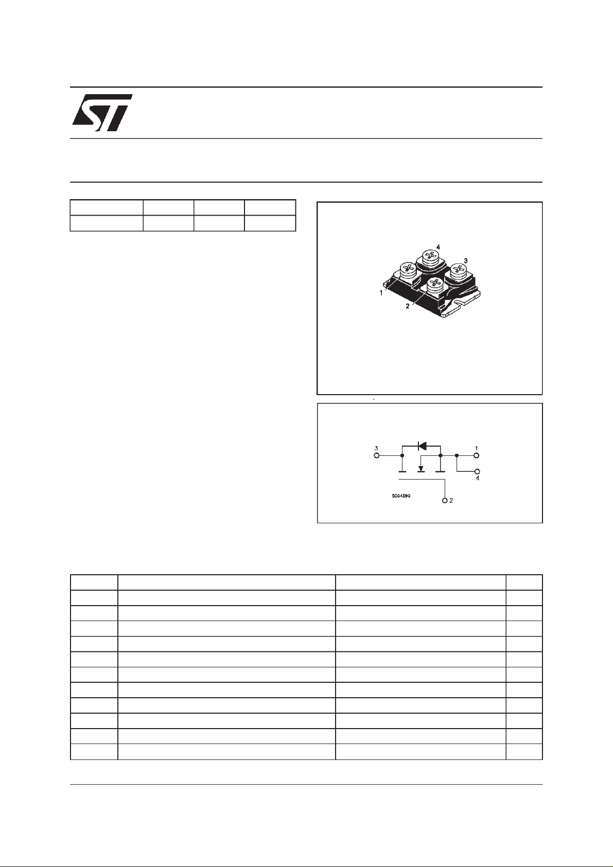
ISOTOP
INTERNAL SCHEMATIC DIAGRAM
ABSOLUTE MAXIMUM RATINGS
Symb o l Parameter Value Unit
V
V
V
I
DM
P
V
T
(•) Pulse width limited by safe operating area (1)ISD≤
February 1999
Drain-source Volt age (VGS= 0) 100 V
DS
Drain- g at e Voltage (RGS=20kΩ) 100 V
DGR
Gate-s ource Voltage
GS
I
Drain Cur rent ( continuous ) at Tc=25oC 180 A
D
I
Drain Cur rent ( continuous ) at Tc=100oC 119 A
D
20 V
±
(•) Drain Cur rent ( pu ls ed) 540 A
Tot al Dissi pat ion at Tc=25oC 450 W
tot
Derat ing F ac tor 3.6 W/
Ins ulat i on Wi t hs t an d Voltage (AC -RMS) 2500 V
ISO
Sto rage Temperat ur e -55 to 15 0
stg
T
Max. Operating Junct ion Temperat ur e 150
j
180
Α,
di/dτ ≤ 200 A/µs, VDD≤ V
(BR)DSS,Tj≤TJMAX
o
C
o
C
o
C
1/8
STE180N10
THERMAL DATA
R
thj-case
R
thc-h
AVALANCHE CHARACTERISTICS
Symbol Parameter Max Value Unit
I
AR
E
Ther mal Resistanc e Junct ion-case Max
Ther mal Resistanc e Case-heatsink W it h conduct ive
Gr ease Applied Max
Avalanche Current, R epetitive or Not-Repetitive
(pulse width limited by T
Single Pul se Avalanc he Ener gy
AS
(starting T
=25oC, ID=IAR,VDD=25V)
j
max)
j
0.27
0.05
60 A
720 mJ
o
C/W
o
C/W
ELECTRICAL CHARACTERISTICS
=25oC unless otherwisespecified)
(T
case
OFF
Symbol Parameter Test Condit ions Min. Typ. M ax. Unit
V
(BR)DSS
Drain-source
ID=1mA VGS= 0 100 V
Break dow n Vo lt age
I
DSS
I
GSS
Zero Gate Voltage
Drain Curre nt (V
GS
Gat e- bod y Leakag e
Current (V
DS
=0)
=0)
V
=MaxRating
DS
=MaxRating Tc= 125oC
V
DS
V
=± 20 V
GS
50
500
400 nA
±
ON(∗)
Symbol Parameter Test Condit ions Min. Typ. M ax. Unit
V
GS(th)
R
DS(on)
Gate Threshold Voltage VDS=VGSID= 250 µA 234V
Sta t ic Drain-s our c e On
VGS=10V ID=90A 5.5 7 m
Resistance
I
D(on)
On State Drain Current VDS>I
D(on)xRDS(on)max
180 A
VGS=10V
DYNAMIC
Symbol Parameter Test Condit ions Min. Typ. M ax. Unit
g
(∗)Forward
fs
Tr ansc on duc tance
C
C
C
Input Capaci t ance
iss
Out put Capac itance
oss
Reverse Transfer
rss
Capacit a nc e
VDS>I
D(on)xRDS(on)maxID
=90A 70 S
VDS=25V f=1MHz VGS=0 18
4
0.5
µ
µA
nF
nF
nF
A
Ω
2/8
STE180N10
ELECTRICAL CHARACTERISTICS
(continued)
SWITCHING ON
Symbol Parameter Test Condit ions Min. Typ. M ax. Unit
t
d(on)
Tur n-on Delay Time
Rise Time
t
r
VDD=50V ID=90A
R
=4.7
G
Ω
VGS=10V
65
230
(Resis t iv e Load, see fig. 3 )
Q
Q
Q
Tot al Gate Charge
g
Gat e- Source Charge
gs
Gate-Drain Charge
gd
VDD=80V ID=180A VGS= 10 V 485
90
210
680 nC
SWITCHING OFF
Symbol Parameter Test Condit ions Min. Typ. M ax. Unit
t
d(on)
Tur n-of f Dela y Tim e
t
Fall T ime
r
VDD=50V ID=90A
=4.7 Ω VGS=10V
R
G
280
100
(Resis t iv e Load, see fig. 3 )
t
r(Voff)
t
t
Off-voltage Rise Time
Fall T ime
f
Cross-over Tim e
c
VDD=80V ID=180A
=4.7 Ω VGS=10V
R
G
(Indu ct iv e Load, see fig. 5)
100
170
260
SOURCEDRAINDIODE
Symbol Parameter Test Condit ions Min. Typ. M ax. Unit
I
SDM
V
I
SD
Q
I
RRM
SD
t
Source-drain Current
(•)
Source-drain Current
180
540
(pulsed)
(∗)ForwardOnVoltage ISD= 180 A VGS=0 1.5 V
Reverse Recovery
rr
Time
Reverse Recovery
rr
ISD= 180 A di/ d t = 100 A/µs
=50V Tj= 150oC
V
DD
(see test circuit, fig. 5)
250
1875
Charge
Reverse Recovery
15
Current
ns
ns
nC
nC
ns
ns
ns
ns
ns
A
A
ns
µC
A
(∗) Pulsed: Pulse duration = 300 µs, duty cycle 1.5 %
(•) Pulse width limited by safe operating area
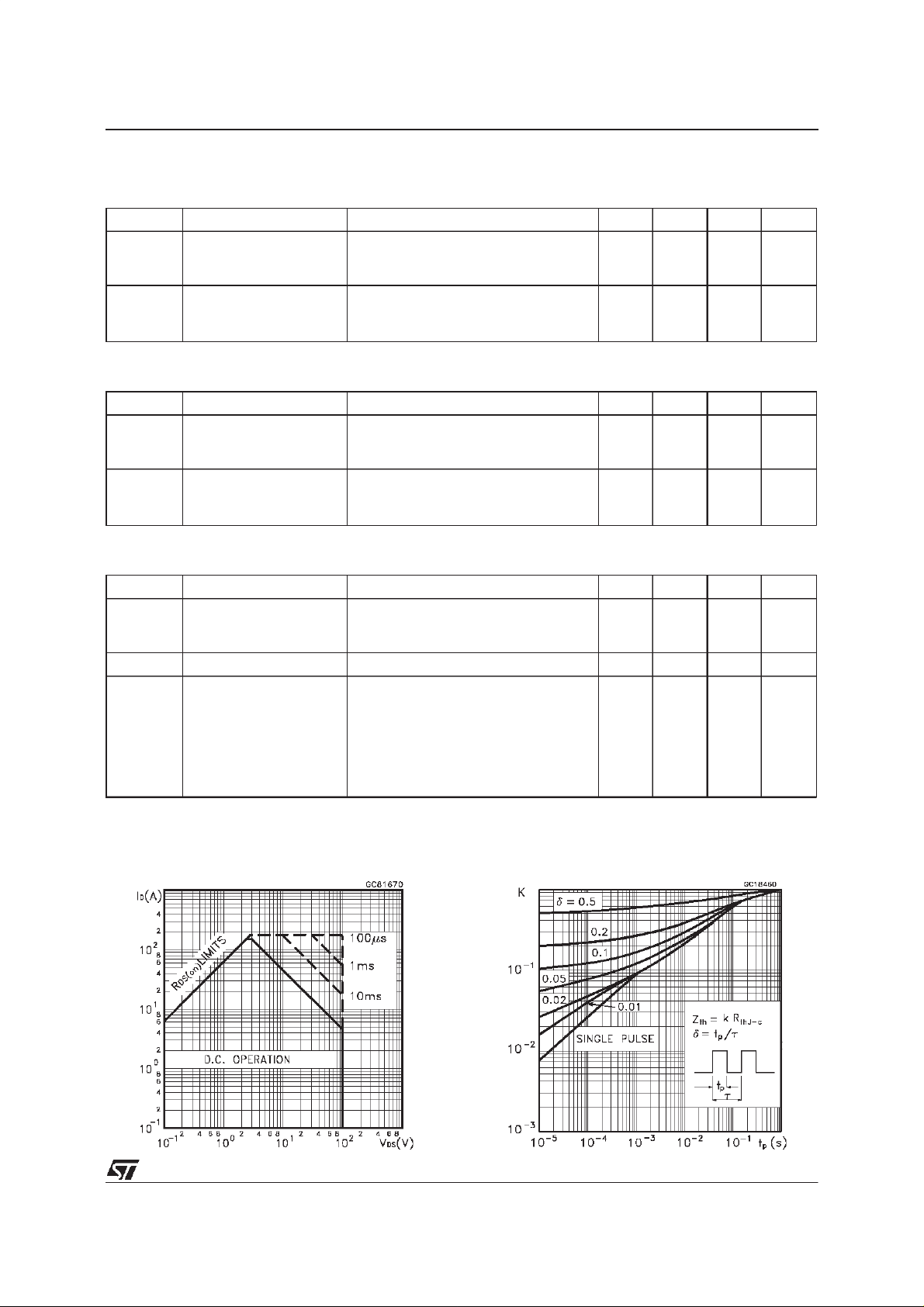
SafeOperating Area ThermalImpedance
3/8
 Loading...