

SGS Thomson Microelectronics STE110NA20 Datasheet
N - CHANNEL ENHANCEMENT MODE
FAST POWER MOS TRANSISTOR
TYPE V
DSS
STE11 0NA 20 200 V < 0.019 Ω 110 A
R
DS(on)
I
D
STE110NA20
PRELIMINARY DATA
■ TYPICALR
■ HIGH CURRENTPOWER MODULE
■ AVALANCHERUGGEDTECHNOLOGY
■ VERYLARGE SOA - LARGE PEAK POWER
DS(on)
=0.015 Ω
CAPABILITY
■ EASY TO MOUNT
■ SAMECURRENT CAPABILITYFOR THE
TWOSOURCE TERMINALS
■ EXTREMELYLOW Rth (Junction to case)
■ VERYLOW INTERNALPARASITIC
INDUCTANCE
■ ISOLATEDPACKAGE UL RECOGNIZED
APPLICATIONS
■ SMPS& UPS
■ MOTORCONTROL
■ WELDINGEQUIPMENT
■ OUTPUTSTAGE FOR PWM, ULTRASONIC
CIRCUITS
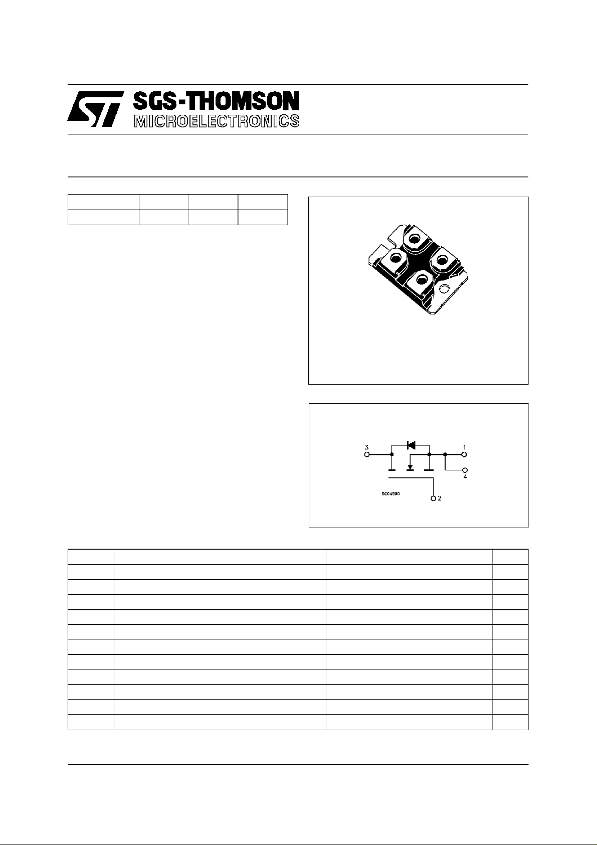
ISOTOP
INTERNAL SCHEMATIC DIAGRAM
ABSOLUTE MAXIMUM RATINGS
Symbol Parameter Value Unit
V
V
V
I
DM
P
T
V
(•) Pulse width limited bysafe operatingarea
March 1996
Drain-source Voltage ( VGS= 0 ) 200 V
DS
Drain- gate Volt age (RGS=20kΩ) 200 V
DGR
Gat e- source Voltage ± 30 V
GS
I
Drain Curren t (co nt inu ous ) at Tc=25oC 110 A
D
I
Drain Curren t (co nt inu ous ) at Tc=100oC73A
D
(•) Drain Current (pulsed) 440 A
Tot al Dissipation at Tc=25oC 450 W
tot
Derating Factor 3.6 W/
St orage Temperatur e -55 to 150
stg
T
Max. Operating Junction Temperatur e 150
j
Ins ulation Withhstand V o lt age (A C- R M S) 2500 V
ISO
o
C
o
C
o
C
1/8
STE110NA20
THERMAL DATA
R
thj-case
R
thc-h
AVALANCHE CHARACTERISTICS
Symb o l Para met er M ax Value Uni t
I
AR
E
E
I
AR
Ther mal Resistance Junct ion-case Max
Ther mal Resistance Case-heatsink Wit h Conduct ive
Gr ease Appli ed Max
Avalanche Current , Repet it iv e or Not-Repe t it ive
(pulse width limi t ed by T
Single Pu lse Avalanc he E nerg y
AS
(starti ng T
Repetitive Avalanche Energy
AR
=25oC, ID=IAR,VDD=50V)
j
(pulse width limi t ed by T
max, δ <1%)
j
max, δ <1%)
j
Avalanche Current , Repet it iv e or Not-Repe t it ive
=100oC, p ulse wid t h limited by Tjmax, δ <1%)
(T
c
0.27
0.05
55 A
500 mJ
175 mJ
32.5 A
o
C/W
o
C/W
ELECTRICAL CHARACTERISTICS (T
=25oC unlessotherwise specified)
case
OFF
Symbol Parameter Test Condition s Min. Typ. Max. Unit
V
(BR)DSS
Drain-source
ID=1mA VGS= 0 200 V
Break dow n Voltage
I
I
DSS
GSS
Zero Gate Voltage
Drain Current (V
GS
Gat e- bod y Leaka ge
Current (V
DS
=0)
=0)
V
=MaxRating
DS
=MaxRatingx0.8 Tc= 125oC
V
DS
V
= ± 30 V ± 400 nA
GS
400
200
ON (∗)
Symbol Parameter Test Condition s Min. Typ. Max. Unit
V
GS(th )
R
DS(on)
I
D(on)
Gat e Thre shold Volt age VDS=VGSID=1mA 2.25 3 3.75 V
St at ic Drain-source On
Resistance
VGS= 10V ID=55A
= 10V ID=55A Tc=100oC
V
GS
On State Drain Current VDS>I
D(on)xRDS(on)max
110 A
0.015 0.019 Ω
VGS=10V
DYNAMIC
Symbol Parameter Test Condition s Min. Typ. Max. Unit
g
(∗)Forward
fs
Tr ansc on ductance
C
C
C
Input Capac it an ce
iss
Out put Capac itance
oss
Reverse Transfer
rss
Capacit a nc e
VDS=15 V ID=55A 38 S
VDS=25V f=1MHz VGS= 0 12.9
2870
980
µA
mA
Ω
nF
pF
pF
2/8
STE110NA20
ELECTRICAL CHARACTERISTICS (continued)
SWITCHINGON
Symbol Parameter Test Condition s Min. Typ. Max. Unit
t
d(on)
t
r
Turn-on Time
Rise Time
VDD=100V ID=55A
=4.7 Ω VGS=10V
R
G
(see test cir cuit, figure 3)
(di/dt)
Tur n-on C urr ent Slope VDD=160V ID= 110 A
on
R
=47 Ω VGS=10V
G
(see tes t circuit, f igure 5)
Q
Q
Q
Tot al Gat e Charge
g
Gate-Source Charge
gs
Gat e- Drain Charge
gd
VDD=160V ID= 110 A VGS= 10 V 470
SWITCHINGOFF
Symbol Parameter Test Condition s Min. Typ. Max. Unit
t
r(Voff)
t
Off -voltage Rise Time
t
Fall T ime
f
Cross-over Time
c
VDD=160V ID= 110 A
=4.7 Ω VGS=10V
R
G
(see test cir cuit, figure 5)
SOURCE DRAIN DIODE
70
95
100
125
290 A/ µs
600 nC
43
226
115
68
160
150
100
210
ns
ns
nC
nC
ns
ns
ns
Symbol Parameter Test Condition s Min. Typ. Max. Unit
I
I
SDM
SD
Source-drain Current
(•)
Source-drain Current
110
440
(pulsed)
(∗)ForwardOnVoltage ISD=110A VGS=0 1.6 V
V
SD
t
Q
Reverse Recovery
rr
Time
Reverse Recovery
rr
ISD= 110 A di/dt = 100 A/µs
=50V Tj=150oC
V
R
(see test cir cuit, figure 5)
625
11
Charge
I
RRM
Reverse Recovery
35
Current
(∗) Pulsed: Pulse duration =300 µs,duty cycle 1.5 %
(•) Pulse width limited by safe operating area
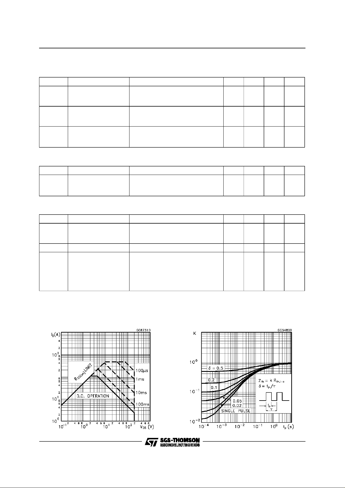
Safe Operating Area ThermalImpedance
A
A
ns
µC
A
3/8
 Loading...