

SGS Thomson Microelectronics STE10-100A Datasheet
1/66
STE10/100A
December 1999
This is preliminary information on a new product now in development. Details are subject to change without notice.
1.0 DESCRIPTION
The STE10/100 is a high performance PCI Fast
Ethernet controller with int egrated physical layer i nterface for 10BASE-T and 100BASE-TX application.
It was designed with advanced CMOS technology to
provide glueless 32-bit bus mast er interface for PCI
bus, boot ROM interface, CSMA/CD protocol for Fast
Ethernet, as well as the physical media interface for
100BASE-TX of IEEE802.3u and 10BASE-T of
IEEE802.3. The auto-negotiation function is also
supported for speed and duplex detection.
The STE10/100 provides both half-duplex and fullduplex operation, as well as support for full-duplex
flow control. It provides long FIFO buffers for transmission and receiving, and early interrupt mechanism to enhance performance. The STE10/100 also
supports ACPI and PCI compliant power management function.
2.0 FEATURES
2.1 Industry standard
■ IEEE802.3u 100BASE-TX and IEEE802.3
10BASE-T compliant
■ Support for IEEE802.3x flow control
■ IEEE802.3u Auto-Negotiation support for
10BASE-T and 100BASE-TX
■ PCI bus interface Rev. 2.2 compliant
■ ACPI and PCI power management standard
compliant
■ Support PC99 wake on LAN
2.2 FIFO
■ Provides independent transmission and
receiving FIFOs, each 2k bytes long
■ Pre- fe tches u p to two tra n smit pa c kets to
minimize inter frame gap (IFG) to 0.96us
■ Retransmits collided packet without reload from
host memory within 64 bytes.
■ Automatically retransmits FIFO under-run
packet with maximum drain threshold until 3rd
time retry failure without influencing the
registers and transmit threshold of next packet.
PQFP128 (14x20x2.7mm)
ORDERING NUMBER: STE10/100A
PRODUCT PREVIEW
PCI 10/100 ETHERNET CONTROLLER
WITH INTEGRATED PHY (3.3V)
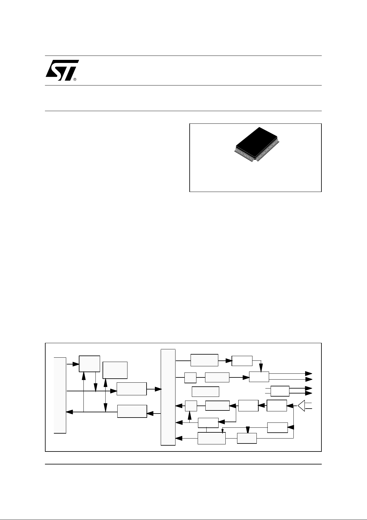
Figure 1. STE10/100Block Diagram
Tx FiFo
DMA
Flow
Control
Manchester
Encoder
Manchester
Decoder
MII
Controller
10 TX
Filter
100 clock
Recovery
10 clock
Recovery
BaseLine
Restore
Adaptive
Equalization
TX Freq.
Synth.
Transmitter
Scrambler
Descrambler
Auto
Negotiation
4B/5B
5B/4B
+
_
Link
Polarity
25Mhz
125Mhz
20Mhz
MAC SubL ay e
MII Controlle r
Rx FiFo
PCI Controller

STE10/100A
2/66
2.3 PCI I/F
■ Provides 32-bit PCI bus master data transfer
■ Supports PCI clock with frequency from 0Hz to 33MHz
■ Supports network operation with PCI system clock from 20MHz to 33MHz
■ Provides performance meter and PCI bus master latency timer for tuning the threshold to enhance the
performance
■ Provides burst transmit packet interrupt and transmit/receive early interrupt to reduce host CPU
utilization
■ As bus master, supports memory-read, memory-read-line, memory-read-multiple, memory-write,
memory-write-and-invalidate command
■ Supports big or little endian byte ordering
2.4 EEPROM/Boot ROM I/F
■ Provides writeable Flash ROM and EPROM as boot ROM, up to 128kB
■ Provides PCI to access boot ROM by byte, word, or double word
■ Re-writes Flash boot ROM through I/O port by programming register
■ Provides serial interface for read/write 93C46 EEPROM
■ Automatically loads device ID, vendor ID, subsystem ID, subsystem vendor ID, Maximum-Latency , and
Minimum-Grand from the 64 byte contents of 93C46 after PCI reset de-asserted
2.5 MAC/Physical
■ Integrates the complete set of Physical layer 100BASE-TX and 10BASE-T functions
■ Provides Full-duplex operation in both 100Mbps and 10Mbps modes
■ Provides Auto-negotiation (NWAY) function of full/half duplex operation for both 10 and 100 Mbps
■ Provides MLT-3 transceiver with DC restoration for Base-line wander compensation
■ Provides transmit wave-shaper, receive filters, and adaptive equalizer
■ Provides MAC and Transceiver (TXCVR) loop-back modes for diagnostic
■ Built-in Stream Cipher Scrambler/ De-scrambler and 4B/5B encoder/decoder
■ Supports external transmit transformer with 1.414:1 turn ratio
■ Supports external receive transformer with 1:1 turn ratio
2.6 LED Display
■ Provides 2 LED display modes:
3 LED displays for
100Mbps (on) or 10Mbps (off)
Link (Remains on when link ok) or Activity (Blinks at 10Hz when receiving or transmitti ng collision-f ree)
FD (Remains on when in Full duplex mode) or when collision detected (Blinks at 20Hz)
4 LED displays for
100 Link (On when 100M link ok)
10 Link (On when 10M link ok)
Activity (Blinks at 10Hz when receiving or transmitting)
FD (Remains on when in Full duplex mode) or when collision detected (Blinks at 20Hz)
3/66
STE10/100A
2.7 Miscellaneous
■ ACPI and PCI compliant power management functions offer significant power-savings performance
■ Provides general purpose timers
■ 128-pin QFP package
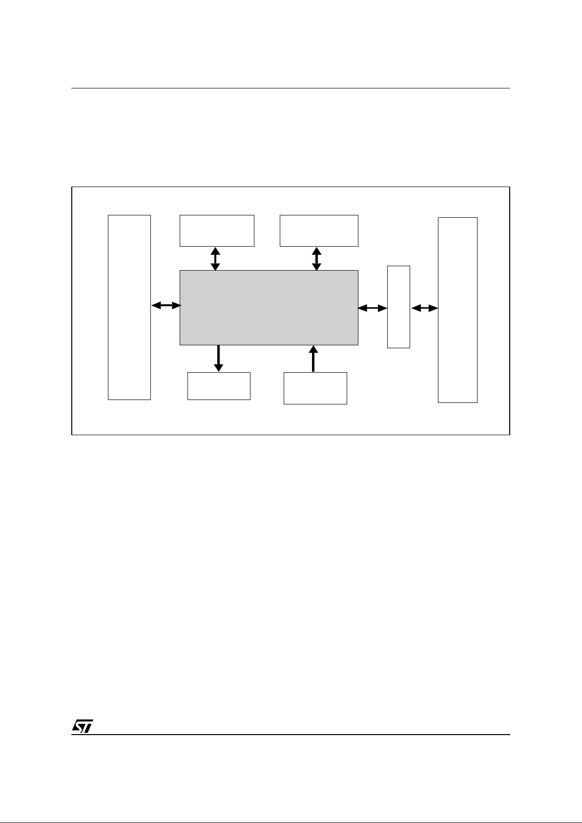
Figure 2. System Diagram of the STE10/100
STE10/100
Serial
EEPROM
Boot ROM
LEDs
25 MHz
Crystal
Xfmr Medium
PCI
Interface

STE10/100A
4/66
3.0 PIN ASSIGNEMENT DIAGRAM
Figure 3. Pin Connection
1
2
3
5
6
4
7
8
9
10
43
11
44 45 46 47 48
123122121120 118119 117116115114113
91
90
89
87
86
88
96
95
94
92
93
AD-23
V
SS
-PCI
IDSEL
AD-24
AD-25
C-BEB3
V
SS
-PCI
AD-20
AD-21
AD-22
V
DD
-PCI
V
SS
-IR
V
DD
-PCI
AD-8
AD-7
C-BEB0
AD-6
V
SS
-PCI
AD-5
AD-4
V
DD
-PCI
AD-29
V
DD
-PCI
AD-30
AD-31
REQ#
PME#
GNT#
PCI-CLK
V
SS
-PCI
RST#
INTA#
LED M1/M2
LED M1/M2
V
CC
-detect
BrA-16/LED M2
BrA-15
V
CC
-detect
AVSSX
AV
DD
REC
AV
SS
REC
LED M1/M2
V
SS
-IR
97
102
101
100
98
99
X2
AV
SS
I
I
REF
AVDDI
X1
AV
DD
X
D99TL443
39 40 41 42
124
AD-28
125
V
SS
-PCI
126
AD-27
127
AD-26
128
V
DD
-PCI
85
84
82
81
83
V
DD
-IR
BrA-14
BrA-12
BrA-11
BrA-13
12
13
14
15
16AD-16
AD-17
V
DD
-PCI
AD-19
AD-18
51
52 53 54 55 56
112 110111 109108107106105
AD-3
V
SS
-PCI
AD-2
AD-1
AD-0
N.C.
V
SS
-IR
BrA -0
V
SS
-IR
AV
SS
T
V
DD
-IR
TX-
AV
DD
T
TX+
AV
SS
R
RX+
49 50
17
18
19
79
78
80
V
SS
-PCI
FRAME#
C-BEB2
BrWE#
BrOE#
BrA-10
77
76
74
73
75
BrCS#
EECS
BrD-7/ECK
BrD-6/EDI
V
SS
-IR
20
21
22
23
24PERR#
STOP#
DEVSEL#
IRDY#
TRDY#
25
26
27
71
70
72
V
DD
-PCI
PAR
SERR#
BrD-4
BrD-3
BrD-5/EDO
69
68
66
65
67
BrD-2
BrD-1
BrA-9
BrA-8
BrD-0
28
29
30
31
32AD-13
V
SS
-PCI
AD-14
C-BEB1
AD-15
33AD-12
34
35
36
37
38V
DD
-IR
AD-9
V
SS
-PCI
AD-11
AD-10
59 60 61 62 63 64
104103
BrA-1
BrA-3
BrA-2
V
DD
-IR
BrA-4
BrA-5
BrA6
BrA-7
RX-
AV
DD
R
57 58

5/66
STE10/100A
4.0 4. PIN DESCRIPTION
Table 1. Pin Description
Pin No. Name Type Description
PCI bus Interface
113 INTA# O/D PCI interrupt request. STE10/100 asserts this signal when one of the interrupt
event is set.
114 RST# I PCI Reset signal to initialize the STE10/100. The RST signal should be asserted
for at least 100µs to ensure that the STE10/100 completes initialization. During
the reset period, all the output pins of STE10/100 will be placed in a highimpedance state and all the O/D pins are floated.
116 PCI-CLK I PCI clock input to STE10/100 for PCI Bus functions. The Bus signals are
synchronized relative to the rising edge of PCI-CLK PCI-CLK must operate at a
frequency in the range between 20MHz and 33MHz to ensure proper network
operation
117 GNT# I PCI Bus Granted. This signal indicates that the STE10/100 has been granted
ownership of the PCI Bus as a result of a Bus Request.
118 REQ# O PCI Bus Request. STE10/100 asserts this line when it needs access to the PCI
Bus.
119 PME# O
OD
The Power Management Event signal is an open drain, active low signal. The
STE10/100 will assert PME# to indicate that a power management event has
occurred.
When WOL (bit 18 of CSR18) is set, the STE10/100 is placed in Wake On LAN
mode. While in this mode, the STE10/100 will activate the PME# signal upon
receipt of a Magic Packet frame from the network.
In the Wake On LAN mode, when LWS (bit 17 of CSR18) is set, the LAN-WAKE
signal follows HP’s protocol; otherwise, it is IBM protocol.
120,121
123,124
126,127
1,2
6,7
9,10
12,13
15,16
29,30
32~35
37
41
43,44
46,47
49,50
52,53
AD-31,30
AD-29,28
AD-27,26
AD-25,24
AD-23,22
AD-21,20
AD-19,18
AD-17,16
AD-15,14
AD-13~10
AD-9
AD-8
AD-7, 6
AD-5,4
AD-3,2
AD-1,0
I/O Multiplexed PCI Bus address/data pins
3
17
28
42
C-BEB3
C-BEB2
C-BEB1
C-BEB0
I/O Bus command and byte enable
4 IDSEL I Initialization Device Select. This signal is asserted when the host issues
configuration cycles to the STE10/100.
18 FRAME# I/O Asserted by PCI Bus master during bus tenure
20 IRDY# I/O Master device is ready to begin data transaction

STE10/100A
6/66
21 TRDY# I/O Target device is ready to begin data transaction
22 DEVSEL# I/O Device select. Indicates that a PCI target device address has been decoded
23 STOP# I/O PCI target device request to the PCI master to stop the current transaction
24 PERR# I/O Data parity error detected, driven by the device receiving data
25 SERR# O/D Address parity error
26 PAR I/O Parity. Even parity computed for AD[31:0] and C/BE[3:0]; master drives PAR for
address and write data phase, target drives PAR for read data phase
BootROM/EEPROM Interface
56~59
61~66
80~86
87
BrA0~3
BrA4~9
BrA10~15
BrA16/
LED M2 -
Fd/Col
I/O ROM data bus
Provides up to 128kB EPROM or Flash-ROM application space.
This pin can be programmed as mode 2 LED display for Full Duplex or Collision
status. It will be driven (LED on) continually when a full duplex configuration is
detected, or it will be driven at a 20 Hz blinking frequency when a collision status
is detected in the half duplex configuration.
67~71
72
73
74
BrD0~4
BrD5/EDO
BrD6/EDI
BrD7/ECK
O
O/I
O/O
O/O
BootROM data bus (0~7)
EDO: Data output of serial EEPROM, data input to STE10/100
EDI:Data input to serial EEPROM, data output from STE10/100
ECK:Clock input to serial EEPROM, sourced by STE10/100
76 EECS O Chip Select of serial EEPROM
77 BrCS# O BootROM Chip Selec t
78 BrOE# O BootROM Read Output Enable for flash ROM application
79 BrWE# O BootROM Write Enable for flash ROM application.
Physical Interface
98 X1 I 25 MHz reference clock input for Physical portion. When an external 25 MHz
crystal is used, this pin will be connected to one of its terminals, and X2 will be
connected to the other terminal. If an external 25 MHz oscillator is used, then this
pin will be connected to the oscillator’s output pin.
97 X2 O 25 MHz reference clock output for Physical portion. When an external 25MHz
crystal is used, this pin will be connected to one of the crystal terminals (see X1,
above). If an external clock source is used, then this pin should be left open.
107,109 TX+, TX- O The differential Transmit outputs of 100BASE-TX or 10BASE-T, these pins
connect directly to Magnetic.
105,104 RX+, RX- I The differential Receive inputs of 100BASE-TX or 10BASE-T, these pins connect
directly from Magnetic.
101 Iref O Reference Resistor connecting pin for reference current, directly connects a 5K
Ohm ± 1% resistor to Vss.
Table 1. Pin Description
Pin No. Name Type Description

7/66
STE10/100A
LED display & Miscellaneous
90 LED M1-
LK/Act
or
LED M2-
Act
O This pin can be programmed as mode 1 or mode 2:
For mode 1:
LED display for Link and Activity status. This pin will be driven on continually
when a good Link test is detected. This pin will be driven at a 10 Hz blinking
frequency when either effective receiving or transmitting is detected.
For mode 2:
LED display for Activity status. This pin will be driven at a 10 Hz blinking
frequency when either effective receiving or transmitting is detected.
92 LED M1-
Speed
or
LED M2-
100 Link
O This pin can be programmed as mode 1 or mode 2:
For mode 1:
LED display for 100M b/s or 10M b/s speed. This pin will be driven on continually
when the 100M b/s network operating speed is detected.
For mode 2:
LED display for 100Ms/s link status. This pin will be driven on continually when
100Mb/s network operating spped is detected.
91 LED M1-
Fd/Col
or
LED M2-
10 Link
O This pin can be programmed as mode 1 or mode 2:
For mode 1:
LED display for Full Duplex or Collision status. This pin will be driven on
continually when a full duplex configuration is detected. This pin will be driven at
a 20 Hz blinking frequency when a collision status is detected in the half duplex
configuration.
For mode 2:
LED display for 10Ms/s link status. This pin will be driven on continually when
10Mb/s network operating speed is detected.
89 Vaux-
detect
I When this pin is asserted, it indicates an auxiliary power source is supported from
the system.
88 Vcc-detect I When this pin is asserted, it indicates a PCI power source is supported.
Digital Power Pins
5,11,19,31,36,39,45,51,55,75,93,112,115,125 Vss
8,14,27,38,40,48,60,85,111,122,128 Vdd
Analog Power Pins
94,96,102,106,110 AVss
95,99,100,103,108 AVdd
Table 1. Pin Description
Pin No. Name Type Description

STE10/100A
8/66
5.0 REGISTERS AND DESCRIPTORS DESCRIPTION
There are three kinds of registers within the STE10/100: STE10/100 configuration registers, PCI control/status
registers, and Transceiver control/status registers.
The STE10/100 configuration regis ters are used to ini tiali ze and confi gure the STE10/100 and for i dentifying
and querying the STE10/100.
The PCI control/status registers are used to communicate between the host and STE10/100. The host can initialize, control, and read the status of the STE10/100 through mapped I/O or memory address space.
The STE10/100 contains 11 16-bit registers to supported Transceiver control and status. They include 7 basic
registers which are defined according to clause 22 “Reconciliation Sub-layer and Media Independent Interface”
and clause 28 “Physical Layer link signaling for 10 Mb/s and 100 Mb/s Auto-Negotiation on twisted pair” of the
IEEE802.3u standard. In addition, 4 special registers are provided for advanced chip control and status.
The STE10/100 also provides receive and transmit descriptors for packet buffering and management.
5.1 STE10/100 Configuration Registers
An STE10/100 software driver can i nitiali ze and confi gure the chi p by writing its confi guration regi sters. The
contents of configuration registers are set to their default values upon power-up or whenever a hardware reset
occurs, but their settings remain unchanged whenever a s oftware reset occurs. The configuration registers are
byte, word, and double word accessible.
Table 2. STE10/100 configuration registers list
Offset Index Name Descriptions
00h CR0 LID Loaded device ID and vendor ID
04h CR1 CSC Configuration Status and Command
08h CR2 CC Class Code and revision number
0ch CR3 LT Latency Timer
10h CR4 IOBA IO Base Address
14h CR5 MBA Memory Base Address
2ch CR11 SID Subsystem ID and vendor ID
30h CR12 BRBA Boot ROM Base Address (ROM size = 128KB)
34h CR13 CP Capability Pointer
3ch CR15 CINT Configuration Interrupt
40h CR16 DS driver space for special purpose
80h CR32 SIG Signature of STE10/100
c0h CR48 PMR0 Power Management Register 0
c4h CR49 PMR1 Power Management Register 1

9/66
STE10/100A
Table 3. STE10/100 configuration registers table
Note: * : automatically recalled from EEPROM when PCI reset is deserted
DS(40h), bit15-8, is read/write able register
SIG(80h) is hard wired register, read only
5.1.1 STE10/100 configuration registers des criptions
offset b31 ----------- b16 b15 ---------- b0
00h Device ID* Vendor ID*
04h Status Command
08h Base Class Code Subclass ------ Revision # Step #
0ch ------ ------ Latency timer cache line size
10h Base I/O address
14h Base memory address
18h~
28h
Reserved
2ch Subsystem ID* Subsystem vendor ID*
30h Boot ROM base address
34h Reserved Cap_Ptr
38h Reserved
3ch Max_Lat* Min_Gnt* Interrupt pin Interrupt line
40h Reserved Driver Space Reserved
80h Signature of STE10/100
c0h PMC Next_Item_Ptr Cap_ID
c4h Reserved PMCSR
Table 4. Configuration Registers Descriptions
Bit # Name Descriptions Default Val RW Type
CR0(offset = 00h), LID - Loaded Identification number of Device and Vendor
31~16 LDID Loaded Device ID, the device ID number loaded from serial
EEPROM.
From
EEPROM
R/O
15~0 LVID Loaded Vendor ID, the vendor ID number loaded from serial
EEPROM.
From
EEPROM
R/O
From EEPROM: Loaded from EEPROM
CR1(offset = 04h), CSC - Configuration command and status
31 SPE Status Parity Error.
1: means that STE10/100 detected a parity error. This bit will
be set even if the parity error response (bit 6 of CR1) is
disabled.
0 R/W
30 SES Status System Error.
1: means that STE10/100 asserted the system error pin.
0 R/W

STE10/100A
10/66
29 SMA St atus Maste r Abort.
1: means that STE10/100 received a master abort and has
terminated a master transaction.
0 R/W
28 STA St atus Target Abort.
1: means that STE10/100 received a target abort and has
terminated a master transaction.
0 R/W
27 --- Reserved.
26, 25 SDST Status Device Select Timing. Indicates the timing of the chip’s
assertion of device select.
01: indicates a medium assertion of DEVSEL#
01 R/O
24 SDPR Status Data Parity Report.
1: when three conditions are met:
a. STE10/100 asserted parity error (PERR#) or it detected
parity error asserted by another device.
b. STE10/100 is operating as a bus master.
c. STE10/100’s parity error response bit (bit 6 of CR1) is
enabled.
0 R/W
23 SFBB Status Fast Back-to-Bac k
Always 1, since STE10/100 has the ability to accept fast back
to back transactions.
1 R/O
22~21 --- Reserved.
20 NC New Capabilities. Indicates whether the STE10/100 provides a
list of extended capabilities, such as PCI power management.
1: the STE10/100 provides the PCI management function
0: the STE10/100 doesn’t provide New Capabilities.
Same as
bit 19 of
CSR18
RO
19~ 9 --- Reserved.
8 CSE Command System Error Response
1: enable system error response. The STE10/100 will assert
SERR# when it finds a parity error during the address phase.
0 R/W
7 --- Reserved.
6 CPE Command Parity Error Response
0: disable parity error response. STE10/100 will ignore any
detected parity error and keep on operating. Default value is
0.
1: enable parity error response. STE10/100 will assert system
error (bit 13 of CSR5) when a parity error is detected.
0 R/W
5~ 3 --- Reserved.
2 CMO Command Master Opera tion Ability
0: disable the STE10/100 bus master ability.
1: enable the PCI bus master ability. Default value is 1 for
normal operation.
0 R/W
1 CMSA Command Memory Space Access
0: disable the memory space access ability.
1: enable the memory space access ability.
0 R/W
Table 4. Configuration Registers Descriptions
Bit # Name Descriptions Default Val RW Type

11/66
STE10/100A
0 CIOSA Command I/O Space Access
0: enable the I/O space access ability.
1: disable the I/O space access ability.
0 R/W
R/W: Read and Write able. RO: Read ab le only.
CR2(offset = 08h), CC - Class Code and Revision Number
31~24 BCC Base Class Code. It means STE10/100 is a network controller. 02h RO
23~16 SC Subclass Code. It means STE10/100 is a Fast Ethernet
Controller.
00h RO
15~ 8 --- Reserved.
7 ~ 4 RN Revision Number, identifies the revision number of STE10/
100.
Ah RO
3 ~ 0 SN Step Number, identifies the STE10/100 steps within the
current revision.
1h RO
RO: Read Only.
CR3(offset = 0ch), LT - Latency Timer
31~16 --- Reserved.
15~ 8 LT Latency Timer. This value specifies the latency timer of the
STE10/100
in units of PCI bus clock cycles. Once the STE10/100
asserts FRAME#, the latency timer starts to count. If the
latency timer expires and the STE10/100 is still asserting
FRAME#, the STE10/100 will terminate the data transaction
as soon as its GNT# is removed.
0 R/W
7 ~ 0 CLS Cache Line Size. This value specifies the system cache line
size in units of 32-bit double words(DW). The STE10/100
supports cache line sizes of 8, 16, or 32 DW. CLS is used by
the STE10/100 driver to program the cache alignment bits (bit
14 and 15 of CSR0) which are used for cache oriented PCI
commands, e.g., memory-read-line, memory-read-multiple,
and memory-write-and-invalidate.
0 R/W
CR4(offset = 10h), IOBA - I/O Base Address
31~ 7 IOBA I/O Base Address. This value indicate the base address of PCI
control and status register (CSR0~28), and Transceiver
registers (XR0~10)
0 R/W
6 ~ 1 --- reserved.
0 IOSI I/O Space Indicator.
1: means that the configuration registers map into I/O space.
1RO
CR5(offset = 14h), MBA - Memory Base Address
31~ 7 MBA Memory Base Address. This value indicate the base address
of PCI control and status register(CSR0~28), and Transceiver
registers(XR0~10)
0 R/W
6 ~ 1 --- reserved.
Table 4. Configuration Registers Descriptions
Bit # Name Descriptions Default Val RW Type

STE10/100A
12/66
0 IOSI Memory Space Indicator.
1: means that the configuration registers map into I/O space.
0RO
CR11(offset = 2ch), SID - Subsystem ID.
31~16 SID Subsystem ID. This value is loaded from EEPROM as a result
of power-on or hardware reset.
From
EEPROM
RO
15~ 0 SVID Subsystem Vendor ID. This value is loaded from EEPROM as
a result power-on or hardware reset.
From
EEPROM
RO
CR12(offset = 30h), BRBA - Boot ROM Base Address. This register should be initialized before accessing the
boot ROM space.
31~10 BRBA Boot ROM Base Address. This value indicates the address
mapping of the boot ROM field as well as defining the boot
ROM size. The values of bit 16~10 are set to 0 indicating that
the STE10/100 supports up to 128kB of boot ROM.
X: b31~17
0: b16~10
R/W
RO
9 ~ 1 --- reserved RO R/W R/
W
0 BRE Boot ROM Enable. The STE10/100 will only enable its boot
ROM access if both the memory space access bit (bit 1 of
CR1) and this bit are set to 1.
1: enable Boot ROM. (if bit 1 of CR1 is also set)
0 R/W
CR13(offset = 34h), CP - Capabilities Pointer.
31~8 --- reserved
7~0 CP Capabilities Pointer. C0H RO
CR15(offset = 3ch), CI - Configuration Interrupt
31~24 ML Max_Lat register. This value indicates how often the STE10/
100 needs to access to the PCI bus in units of 250ns. This
value is loaded from serial EEPROM as a result of power-on
or hardware reset.
From
EEPROM
RO
23~16 MG Min_Gnt register. This value indicates how long the STE10/
100 needs to retain the PCI bus ownership whenever it
initiates a transaction, in units of 250ns. This value is loaded
from serial EEPROM as a result power-on or hardware reset.
From
EEPROM
RO
15~ 8 IP Interrupt Pin. This value indicates one of four interrupt request
pins to which the STE10/100 is connected.
01h: means the STE10/100 always connects to INTA#
01h RO
7 ~ 0 IL Interrupt Line. This value indicates the system interrupt
request lines to which the INTA# of STE10/100 is routed. The
BIOS will fill this field when it initializes and configures the
system. The STE10/100 driver can use this value to determine
priority and vector information .
0 R/W
CR16(offset = 40h), DS - Driver Space for special purpose.
31~16 --- reserved
Table 4. Configuration Registers Descriptions
Bit # Name Descriptions Default Val RW Type

13/66
STE10/100A
15~8 DS Driver Space for implementation-specific purpose. Since this
area won’t be cleared upon software reset, an STE10/100
driver can use this R/W area as user-specified storage.
0 R/W
7 ~ 0 --- reserved
CR32(offset = 80h), SIG - Signature of STE10/100
31~16 DID Device ID, the device ID number of the STE10/100. 2774h RO
15~0 VID Vendor ID, the vendor ID number of STMicroelectronics 104Ah RO
CR48(offset = c0h), PMR0, Power Management Register0.
31
30
29
28
27
PSD3c,
PSD3h,
PSD2,
PSD1,
PSD0
PME_Support.
The STE10/100 will assert PME# signal while in the D0, D1,
D2, D3hot and D3cold power state. The STE10/100 supports
Wake-up from the above five states. Bit 31 (support wake-up
from D3cold) is loaded from EEPROM after power-up or
hardware reset. To support the D3cold wake-up function, an
auxiliary power source will be sensed during reset by the
STE10/100 Vaux_detect pin. If sensed low, PSD3c will be set
to 0; if sensed high, and if D3CS (bit 31of CSR18) is set
(CSR18 bits 16~31 are recalled from EEPROM at reset), then
bit 31 will be set to 1.
X1111b RO
26 D2S D2_Support. The STE10/100 supports the D2 Power
Management State.
1RO
25 D1S D1_Support. The STE10/100 supports the D1 Power
Management State.
1RO
24~22 AUXC Aux Current. These three bits report the maximum 3.3Vaux
current requirements for STE10/100 chip. If bit 31 of PMR0 is
‘1’, the default value is 111b, meaning the STE10/100 needs
375 mA to support remote wake-up in D3cold power state.
Otherwise, the default value is 000b, meaning the STE10/100
does not support remote wake-up from D3cold power state.
XXXb RO
21 DSI The Device Specific Initialization bit indicates whether any
special initialization of this function is required before the
generic class device driver is able to use it.
0: indicates that the function does not require a device-specific
initialization sequence following transition to the D0
uninitialized state.
0RO
20 --- Reserved.
19 PMEC PME Clock. Indicates that the STE10/100 does not rely on the
presence of the PCI clock for PME# operation
0RO
18~16 VER Version. The value of 010b indicates that the STE10/100
complies with Revision 1.0a of the PCI Power Management
Interface Specification.
010b RO
15~8 NIP Next Item Pointer. This value is always 0h, indicating that
there are no additional items in the Capabilities List.
00h RO
7~0 CAPID Capability Identifier. This value is always 01h, indicating the
link list item as being the PCI Power Management Registers.
01h RO
Table 4. Configuration Registers Descriptions
Bit # Name Descriptions Default Val RW Type

STE10/100A
14/66
CR49(offset = c4h), PMR1, Power Management Register 1.
31~16 --- reserved
15 PMEST PME_Status. This bit is set whenever the STE10/100 detects
a wake-up event, regardless of the state of the PME-En bit.
Writing a “1” to this bit will clear it, causing the STE10/100 to
deassert PME# (if so enabled). Writing a “0” has no effect.
If PSD3c (bit 31 of PMR0) is cleared (i.e. it does not support
PME# generation from D3cold), this bit is by default 0;
otherwise, PMEST is cleared upon power-up reset only and is
not modified by either hardware or software reset.
X R/W1C*
14,13 DSCAL Data_Scale. Indicates the scaling factor to be used when
interpreting the value of the Data register. This field is
required for any function that implements the Data register.
The STE10/100 does not support Data register and
Data_Scale.
00b RO
12~9 DSEL Data_Select. This four bit field is used to select which data is
to be reported through the Data register and Data_Scale field.
This field is required for any function that implements the Data
register.
The STE10/100 does not support Data_select.
0000b R/W
8 PME_En PME_En. When set, enables the STE10/100 to assert PME#.
When cleared, disables the PME# assertion.
If PSD3c (bit 31 of PMR0) is cleared (i.e. it does not support
PME# generation from D3cold), this bit is by default 0;
otherwise, PME_En is cleared upon power up reset only and is
not modified by either hardware or software reset.
X R/W
7~2 --- reserved. 000000b RO
1,0 PWRS PowerState. This two bit field is used both to determine the
current power state of the STE10/100 and to place the STE10/
100 in a new power state. The definition of this field is given
below.
00b - D0
01b - D1
10b - D2
11b - D3hot
If software attempts to write an unsupported state to this field,
the write operation will complete normally on the bus, but the
data is discarded and no state change occurs.
00b R/W
R/W1C*, Read Only and Wri t e one cleared.
Table 4. Configuration Registers Descriptions
Bit # Name Descriptions Default Val RW Type

15/66
STE10/100A
5.2 PCI Control/Status registers
Table 5. PCI Control/Status registers list
offset from base
address of CSR
Index Name Descriptions
00h CSR0 PAR PCI acces s register
08h CSR1 TDR transmit demand register
10h CSR2 RDR receive demand register
18h CSR3 RDB receive descriptor base address
20h CSR4 TDB transmit descriptor base address
28h CSR5 SR status register
30h CSR6 NAR network access register
38h CSR7 IER interrupt enable register
40h CSR8 LPC lost packet counter
48h CSR9 SPR serial port register
50h CSR10 --- Reserved
58h CSR11 TMR Timer
60h CSR12 --- Reserved
68h CSR13 WCSR Wake-up Control/Status Register
70h CSR14 WPDR Wake-up Pattern Data Register
78h CSR15 WTMR watchdog timer
80h CSR16 ACSR5 status register 2
84h CSR17 ACSR7 interrupt enable register 2
88h CSR18 CR command register
8ch CSR19 PCIC PCI bus performance counter
90h CSR20 PMCSR Power Management Comm and and Status
94h CSR21 - -- Reserved
98h CSR22 - -- Reserved
9ch CSR23 TXBR transmit burst counter/time-out register
a0h CSR24 FROM flash(boot) ROM port
a4h CSR25 PAR0 physical address register 0
a8h CSR26 PAR1 physical address register 1
ach CSR27 MAR0 multicast address hash table register 0
b0h CSR28 MAR1 multicast address hash table register 1

STE10/100A
16/66
Table 6. Control/Status register description
Bit # Name Descriptions Default Val RW Type
CSR0(offset = 00h), PAR - PCI Access Register
31~25 --- reserved
24 MWIE Memory Write and Invalidate Enable.
1: enable STE10/100 to generate memory write invalidate
command. The STE10/100 will generate this command
while writing full cache lines.
0: disable generating memory write invalidate command. The
STE10/100 will use memory write commands instead.
0 R/W*
23 MRLE Memory Read Line Enable.
1: enable STE10/100 to generate memory read line command
when read access instruction reaches the cache line
boundary. If the read access instruction doesn’t reach the
cache line boundary then the STE10/100 uses the memory
read command instead.
0 R/W*
22 --- reserved
21 MRME Memory Read Multiple Enable.
1: enable STE10/100 to generate memory read multiple
commands when reading a full cache line. If the memory is
not cache-aligned, the STE10/100 uses the memory read
command instead.
0 R/W*
20~19 --- reserved
18,17 TAP Transmit auto-polling in transmit suspended state.
00: disable auto-polling (default)
01: polling own-bit every 200 us
10: polling own-bit every 800 us
11: polling own-bit every 1600 us
00 R/W*
16 --- reserved
15, 14 CAL Cache alignment. Address boundary for data burst, set after
reset
00: reserved (default)
01: 8 DW boundary alignment
10: 16 DW boundary alignment
11: 32 DW boundary alignment
00 R/W*
13 ~ 8 PBL Programmable Burst Length. This value defines the maximum
number of DW to be transferred in one DMA transaction.
value: 0 (unlimited), 1, 2, 4, 8, 16(default), 32
010000 R/W*
7 BLE Big or Little Endian selection.
0: little endian (e.g. INTEL)
1: big endian (only for data buffer)
0 R/W*
6 ~ 2 DSL Descriptor Skip Length. Defines the gap between two
descriptors in the units of DW.
0 R/W*
1 BAR Bus arbitration
0: receive operations have higher priority
1: transmit operations have higher priority
0 R/W*

17/66
STE10/100A
0 SWR Software reset
1: reset all internal hardware (including MAC and
transceivers), except configuration registers. This signal will
be cleared by the STE10/100 itself after the reset process is
completed.
0 R/W*
R/W* = Before writing the transmit and receive operations should be stopped.
CSR1(offset = 08h), TDR - Transmit demand register
31~ 0 TPDM Transmit poll demand.
While the STE10/100 is in the suspended state, a write to this
register (any value) will trigger the read-tx-descriptor process,
which checks the own-bit; if set, the transmit process is then
started.
FFFFFFFF
h
R/W*
R/W* = Before writing the transmit process should be in the suspended state.
CSR2(offset = 10h), RDR - Receive demand register
31 ~ 0 RPDM Receive poll demand
While the STE10/100 is in the suspended state, a write to this
register (any value) will trigger the read-rx-descriptor process,
which checks the own-bit, if set, the process to move data
from the FIFO to buffer is then started.
FFFFFFFF
h
R/W*
R/W* = Before writing the receive process should be in the suspended state.
CSR3(offset = 18h), RDB - Receive descriptor base address
31~ 2 SAR Start address of receive descriptor 0 R/W*
1, 0 RBND must be 00, DW boundary 00 RO
R/W* = Before writing the receive process should be stopped.
CSR4(offset = 20h), TDB - Transmit descriptor base address
31~ 2 SAT Start address of transmit descriptor 0 R/W*
1, 0 TBND must be 00, DW boundary 00 RO
R/W* = Before writing the transmit process should be stopped.
CSR5(offset = 28h), SR - Status register
31~ 26 ---- reserved
25~ 23 BET Bus Error Type. This field is valid only when bit 13 of
CSR5(fatal bus error) is set. There is no interrupt generated by
this field.
000: parity error, 001: master abort, 010: target abort
011, 1xx: reserved
000 RO
Table 6. Control/Status register description
Bit # Name Descriptions Default Val RW Type

STE10/100A
18/66
22~ 20 TS Transmit State. Reports the current transmission state only, no
interrupt will be generated.
000: stop
001: read descriptor
010: transmitting
011: FIFO fill, read the data from memory and put into FIFO
100: reserved
101: reserved
110: suspended, unavailable transmit descriptor or FIFO
overflow
111: write descriptor
000 RO
19~17 RS Receive State. Reports current receive state only, no interrupt
will be generated.
000: stop
001: read descriptor
010: check this packet and pre-fetch next descriptor
011: wait for receiving data
100: suspended
101: write descriptor
110: flush the current FIFO
111: FIFO drain, move data from receiving FIFO into memory
000 RO
16 NISS Normal Interrupt Status Summary. Set if any of the following
bits of CSR5 are asserted:
TCI, transmit completed interrupt (bit 0)
TDU, transmit descriptor unavailable (bit 2)
RCI, receive completed interrupt (bit 6)
0 RO/LH*
15 AISS Abnormal Interrupt Status Summary. Set if any of the
following bits of CSR5 are asserted:
TPS, transmit process stopped (bit 1)
TJT, transmit jabber timer time-out (bit 3)
TUF, transmit under-flow (bit 5)
RDU, receive descriptor unavailable (bit 7)
RPS, receive process stopped (bit 8)
RWT, receive watchdog time-out (bit 9)
GPTT, general purpose timer time-out (bit 11)
FBE, fatal bus error (bit 13)
0 RO/LH*
14 ---- reserved
13 FBE Fatal Bus Error.
1: on occurrence of parity error, master abort, or target abort
(see bits 25~23 of CSR5). The STE10/100 will disable all bus
access. A software reset is required to recover from a parity
error.
0 RO/LH*
12 --- reserved
11 GPTT General Purpose Timer Timeout, based on CSR11 timer
register
0 RO/LH*
10 --- reserved
9 RWT Receive Watchdog Timeout, based on CSR15 watchdog timer
register
0 RO/LH*
8 RPS Receive Process Stopped, receive state = stop 0 RO/LH*
Table 6. Control/Status register description
Bit # Name Descriptions Default Val RW Type

19/66
STE10/100A
7 RDU Receive Descriptor Unavailable
1: when the next receive descriptor can not be obtained by the
STE10/100. The receive process is suspended in this
situation. To restart the receive process, the ownership bit of
the next receive descriptor should be set to STE10/100 and a
receive poll demand command should be issued (if the receive
poll demand is not issued, the receive process will resume
when a new recognized frame is received).
0 RO/LH*
6 RCI Receive Completed Interrupt
1: when a frame reception is completed.
0 RO/LH*
5 T UF Transmit Unde r-Flow
1: when an under-flow condition occurs in the transmit FIFO
during transmitting. The transmit process will enter the
suspended state and report the under-flow errror on bit 1 of
TDES0.
0 RO/LH*
4 --- Reserved
3 TJT Transmit Jabber Timer Time-out
1: when the transmit jabber timer expires. The transmit
processor will enter the stop state and TO (bit 14 of TDES0,
transmit jabber time-out flag) will be asserted.
0 RO/LH*
2 TDU Transmit Descriptor Unavailable
1: when the next transmit descriptor can not be obtained by
the STE10/100. The transmission process is suspended in this
situation. To restart the transmission process, the ownership
bit of the next transmit descriptor should be set to STE10/100
and, if the transmit automatic polling is not enabled, a transmit
poll demand command should then be issued.
0 RO/LH*
1 T PS Transmit Proce ss Stopped .
1: while transmit state = stop
0 RO/LH*
0 TCI Transmit Completed Interrupt.
1: set when a frame transmission completes with IC (bit 31 of
TDES1) asserted in the first transmit descriptor of the frame.
0 RO/LH*
LH = High Latching and cleared by writing 1.
CSR6(offset = 30h), NAR - Network access register
31~22 --- reserved
21 SF Store and forward for transmit
0: disable
1: enable, ignore the transmit threshold setting
0 R/W*
20 --- reserved
19 SQE SQE Disable
0: enable SQE function for 10BASE-T operation. The STE10/
100 provides SQE test function for 10BASE-T half duplex
operation.
1: disable SQE function.
1 R/W*
18~16 ----- reserved
Table 6. Control/Status register description
Bit # Name Descriptions Default Val RW Type

STE10/100A
20/66
15~14 TR transmit threshold control
00: 128-bytes (100Mbps), 72-bytes (10Mbps)
01: 256-bytes (100Mbps), 96-bytes (10Mbps)
10: 512-bytes (100Mbps), 128-bytes (10Mbps)
11: 1024-bytes (100Mbps), 160-bytes (10Mbps)
00 R/W*
13 ST Stop transmit
0: stop (default)
1: start
0 R/W
12 FC Force collision mode
0: disable
1: generate collision upon transmit (for testing in loop-back
mode)
0 R/W**
11, 10 OM Operating Mode
00: normal
01: MAC loop-back, regardless of contents of XLBEN (bit 14 of
XR0, XCVR loop-back)
10,11: reserved
00 R/W**
9, 8 --- reserved
7 MM Multicast Mode
1: receive all multicast packets
0 R/W***
6 PR Promiscuous Mode
1: receive any good packet.
0: receive only the right destination address packets
1 R/W***
5 SBC Stop Back-off Counter
1: back-off counter stops when carrier is active, and resumes
when carrier is dropped.
0: back-off counter is not effected by carrier
0 R/W**
4 --- reserved
3 PB Pass Bad packet
1: receives any packets passing address filter, including runt
packets, CRC error, truncated packets. For receiving all
bad packets, PR (bit 6 of CSR6) should be set to 1.
0: filters all bad packets
0 R/W***
2 --- reserved
1 SR Start/Stop Receive
0: receive processor will enter stop state after the current
frame reception is completed. This value is effective only
when the receive processor is in the running or suspending
state. Note: In “Stop Receive” state, the PAUSE packet and
Remote Wake Up packet will not be affected and can be
received if the corresponding function is enabled.
1: receive processor will enter running state.
0 R/W
0 --- reserved
W* = only write when the transmit processor stopped.
W** = only wri te when the transmit and receive processor both stopp ed .
W*** = only write when the receive processo r stoppe d.
CSR7(offset = 38h), IER - Interrupt Enable Register
Table 6. Control/Status register description
Bit # Name Descriptions Default Val RW Type
 Loading...