

®
N - CHANNEL 55V - 0.1 Ω - 12A TO-252
TYPE V
DSS
STDID5B 55 V < 0.12 Ω 12 A
■
TYPICAL R
■
APPLICATION ORIENTED
DS(on)
= 0.1 Ω
CHARACTERIZATION
■
ADD SUFFIX "T4" FOR ORDERING IN TAPE
& REEL
DESCRIPTION
This Power MOSFET is the latest development of
STMicroelectronics unique "Single Feature
Size" strip-based process. The resulting transistor shows extremely high packing density for low
on-resistance, rugged avalanche characteristics
and less critical alignment steps therefore a remarkable manufacturing reproducibility.
R
DS(on)
I
D
STDID5B
STripFET POWER MOSFET
PRELIMINARY DATA
3
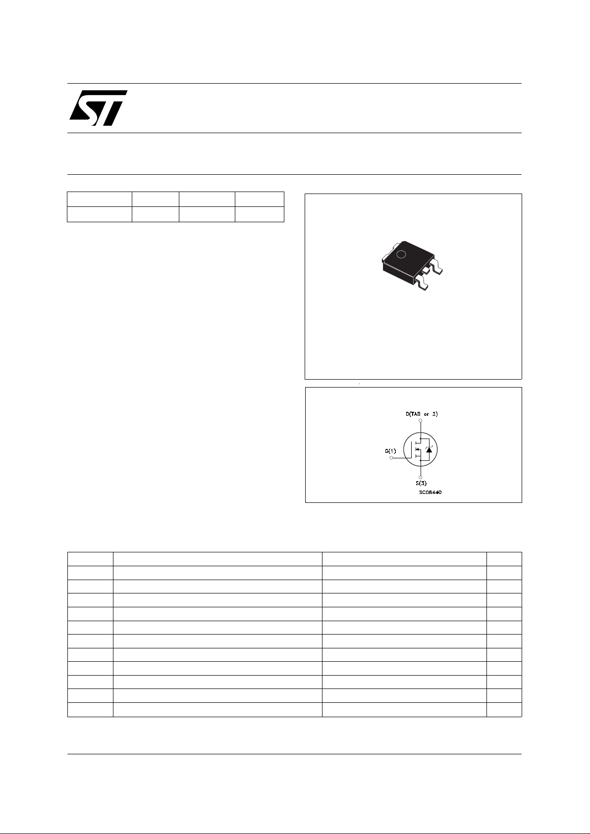
1
DPAK
TO-252
(Suffix "T4")
APPLICATIONS
■
DC MOTOR CONTROL
■
DC-DC & DC-AC CONVERTERS
INTERNAL SCHEMATIC DIAGRAM
ABSOLUTE MAXIMUM RATINGS
Symbol Parameter Value Unit
V
V
V
I
D
I
DM
P
E
AS
T
(•) Pulse width limited by safe operating area
Drain-source Voltage (VGS = 0) 55 V
DS
Drain- gate Voltage (RGS = 20 kΩ)55V
DGR
Gate-source Voltage ± 20 V
GS
(*) Drain Current (continuous) at Tc = 25 oC12A
I
Drain Current (continuous) at Tc = 100 oC8A
D
(•) Drain Current (pulsed) 48 A
Total Dissipation at Tc = 25 oC35W
tot
Derating Factor 0.23 W/
(1)
Single Pulse Avalanche Energy 25 mJ
Storage Temperature -65 to 175
stg
T
Max. Operating Junction Temperature 175
j
(1) starting T
o
C, ID =12A , VDD = 30V New R
= 25
j
spec. starting from July ’98
DS(on)
o
C
o
C
o
C
May 2000
1/6
STDID5B
THERMAL DATA
R
thj-case
R
thj-amb
T
Thermal Resistance Junction-case Max
Thermal Resistance Junction-ambient Max
Maximum Lead Temperature For Soldering Purpose
l
4.3
100
275
o
C/W
o
C/W
o
C
ELECTRICAL CHARACTERISTICS
= 25 oC unless otherwise specified)
(T
case
OFF
Symbol Parameter Test Conditions Min. Typ. Max. Unit
V
(BR)DSS
Drain-source
ID = 250 µA V
= 0 55 V
GS
Breakdown Voltage
I
DSS
I
GSS
Zero Gate Voltage
Drain Current (V
GS
Gate-body Leakage
Current (V
DS
= 0)
= 0)
= Max Rating
V
DS
V
= Max Rating Tc = 125 oC
DS
= ± 20 V ± 100 nA
V
GS
1
10
ON (∗)
Symbol Parameter Test Conditions Min. Typ. Max. Unit
V
GS(th)
R
DS(on)
Gate Threshold Voltage V
Static Drain-source On
= VGS ID = 250 µA234V
DS
VGS = 10 V ID = 9.6 A 0.1 0.12 Ω
Resistance
I
D(on)
On State Drain Current VDS > I
V
= 10 V
GS
D(on)
x R
DS(on)max
12 A
DYNAMIC
Symbol Parameter Test Conditions Min. Typ. Max. Unit
g
(∗) Forward
fs
Transconductance
C
C
C
Input Capacitance
iss
Output Capacitance
oss
Reverse Transfer
rss
Capacitance
VDS > I
V
DS
x R
D(on)
DS(on)max
= 25 V f = 1 MHz V
ID = 10 A 4 S
= 0 V 360
GS
55
25
µA
µA
pF
pF
pF
2/6

STDID5B
ELECTRICAL CHARACTERISTICS (continued)
SWITCHING ON
Symbol Parameter Test Conditions Min. Typ. Max. Unit
t
d(on)
Turn-on Delay Time
Rise Time
t
r
V
= 30 V ID = 6 A
DD
R
= 4.7 Ω VGS = 10 V
G
(Resistive Load, see fig. 3)
Q
Q
Q
Total Gate Charge
g
Gate-Source Charge
gs
Gate-Drain Charge
gd
V
= 48 V ID = 12 A V
DD
= 10 V 10
GS
SWITCHING OFF
Symbol Parameter Test Conditions Min. Typ. Max. Unit
t
d(off)
Turn-off Delay Time
Fall Time
t
f
V
= 30 V ID = 6 A
DD
R
= 4.7 Ω VGS = 10 V
G
(Resistive Load, see fig. 3)
SOURCE DRAIN DIODE
Symbol Parameter Test Conditions Min. Typ. Max. Unit
I
SD
I
SDM
V
SD
t
Q
I
RRM
(∗) Pulsed: Pulse duration = 300 µs, duty cycle 1.5 %
(•) Pulse width limited by safe operating area
Source-drain Current
(•)
Source-drain Current
(pulsed)
(∗) Forward On Voltage ISD = 12 A VGS = 0 1.3 V
Reverse Recovery
rr
Time
Reverse Recovery
rr
I
= 12 A di/dt = 100 A/µs
SD
V
= 30 V Tj = 150 oC
DD
(see test circuit, fig. 5)
Charge
Reverse Recovery
Current
10
25
13.5 nC
3.5
3.2
31
8
12
48
38
61
3.2
ns
ns
nC
nC
ns
ns
A
A
ns
nC
A
3/6

STDID5B
Fig. 1: Unclamped Inductive Load Test Circuit
Fig. 3: Switching Times Test Circuits For
Resistive Load
Fig. 2: Unclamped Inductive Waveform
Fig. 4: Gate Charge test Circuit
Fig. 5: Test Circuit For Inductive Load Switching
And Diode Recovery Times
4/6

TO-252 (DPAK) MECHANICAL DATA
STDID5B
DIM.
mm inch
MIN. TYP. MAX. MIN. TYP. MAX.
A 2.2 2.4 0.086 0.094
A1 0.9 1.1 0.035 0.043
A2 0.03 0.23 0.001 0.009
B 0.64 0.9 0.025 0.035
B2 5.2 5.4 0.204 0.212
C 0.45 0.6 0.017 0.023
C2 0.48 0.6 0.019 0.023
D 6 6.2 0.236 0.244
E 6.4 6.6 0.252 0.260
G 4.4 4.6 0.173 0.181
H 9.35 10.1 0.368 0.397
L2 0.8 0.031
L4 0.6 1 0.023 0.039
A
C2
L2
E
B2
==
H
DETAIL "A"
D
==
C
B
2
1 3
L4
A1
G
==
A2
DETAIL "A"
0068772-B
5/6

STDID5B
Information furnished is believed to be accurate and reliable. However, STMicroelectronics assumes no responsibility for the consequences
of use of such inform ation nor for any in fringe ment o f patents or other rig hts of third par ties wh ich may result from its u se. N o li cen se is
granted by implication or otherwise under any patent or patent rights of STMicroelectronics. Specification mentioned in this publication are
subject to change without notice. This publication supersedes and replaces all information previously supplied. STMicroelectronics products
are not authorized f or use as critical components in life support devices or systems without express written approval of STMicroelectronics.
The ST logo is a trademark of STMicroelectronics
© 2000 STMicroelectro nics – Printed in Italy – All Rights Reserved
STMicroelectronics GROUP OF COMPANIES
Australia - Brazil - China - Finland - France - Germany - Hong Kong - India - Italy - Japan - Malaysia - Malta - Morocco -
Singapore - Spain - Sweden - Switzerland - United Kingdom - U.S.A.
http://www.st.com
6/6
 Loading...