

1/2
DATA BRIEFING
September 2001
This is Brief Data from STMicroelectronics. Details are subject to change without notice. For complete data, please contact
your nearest Sales Office or SmartCard Products Divison, Rousset, France. Fax: (+33) 4 42 68 87 29.
SMARTCARD MCU
Ordering Information
For Package And Delivery
INTRODUCTION
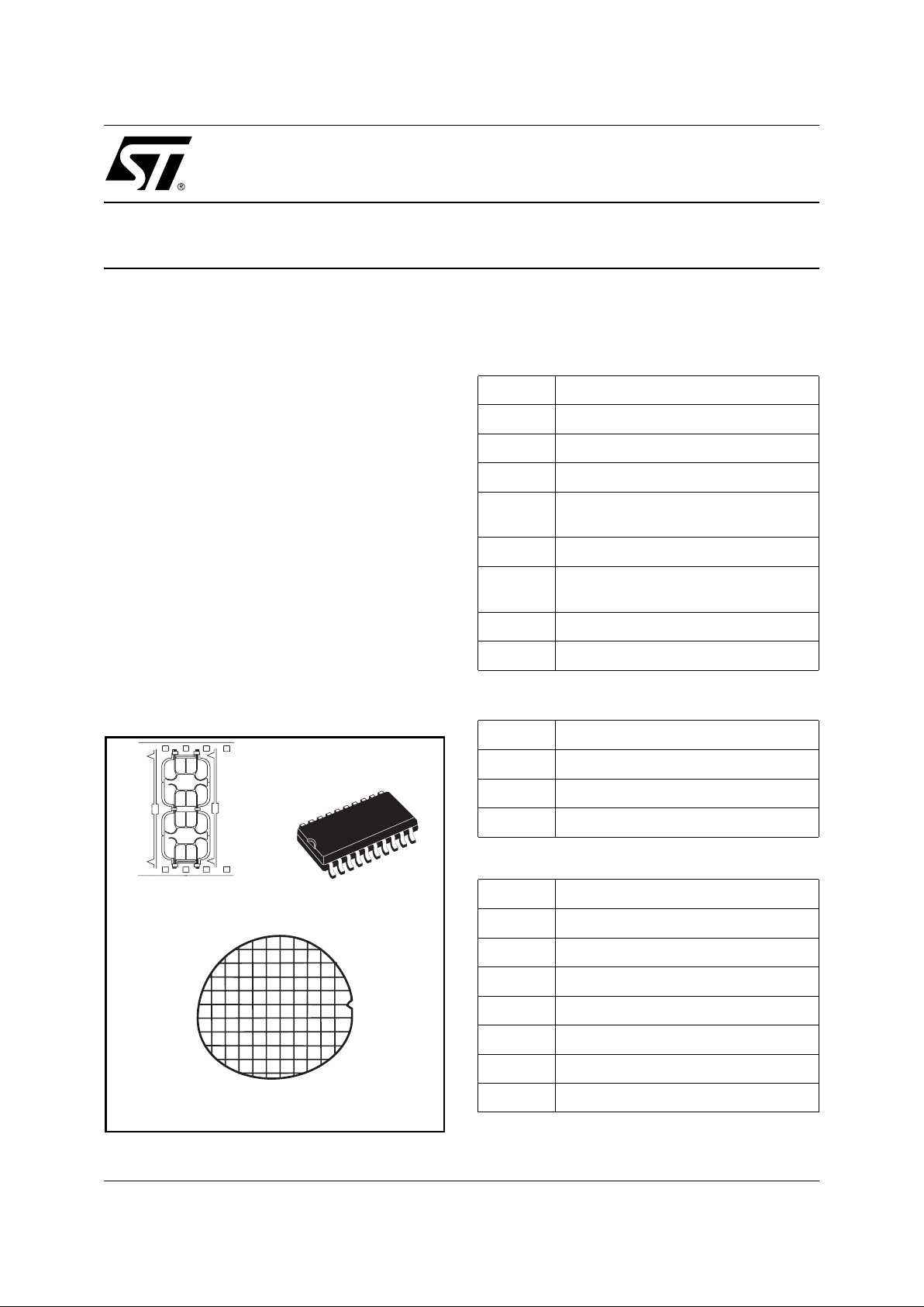
The manufacturing process of Smartcards involves various components and technologies in
order to issue a finished product:
– micromodules,
– flat packages,
– wafers.
■ MICROMODULES
Dedicated package for Smartcard products, the
micromodule type depends on the size of the
product and on the application.
Table 1 lists all available micromodules.
■ FLAT PACKAGES
For applications which require surface mount technology, suitable for PC cards, or other security
modules, STMicroelectronics offers flat packages
listed In Table 2.
■ WAFERS
For issuer production need, ST offers sawn and
unsawn wafers deliveries, listed in Table 3.
Figure 1. Delivery form
Table 1. Micromodules in super 35 stand ard
tape
Table 2. Flat Packages
Table 3. Wafers
4
4
4
4
SO20
261a.ai
8” Wafer
Micromodule
Notch
Type Description
D1, D2 8 contacts for memory cards
D15 6 contacts for memory cards
D3, D4 8 contacts with ring MCU cards
D5
8 contacts for dual contact contactless
MCU cards
D68 8 contacts for MCU cards
D7
6 contacts for dual contact contactless
MCU cards
C7 Full contactless for MCU cards
D8 8 contacts for MCU cards
Type Description
O20 SO20 for MCU products
QF4 TQFP44 for MCU products
R20 SO20 on tape and reel for MCU products
Type Description
W00 Unsawn wafers, 750 µm thickness
W20 Unsawn wafers, 275 µm thickness
W40 Unsawn wafers, 180 µm thickness
S2x 280 µm sawn wafers on UV tape
R4x 180 µm sawn wafers on insolated UV tape
S4x 180 µm sawn wafers on UV tape
T4x 180 µm sawn wafers on blue tape
SMARTCARD MCU
2/2
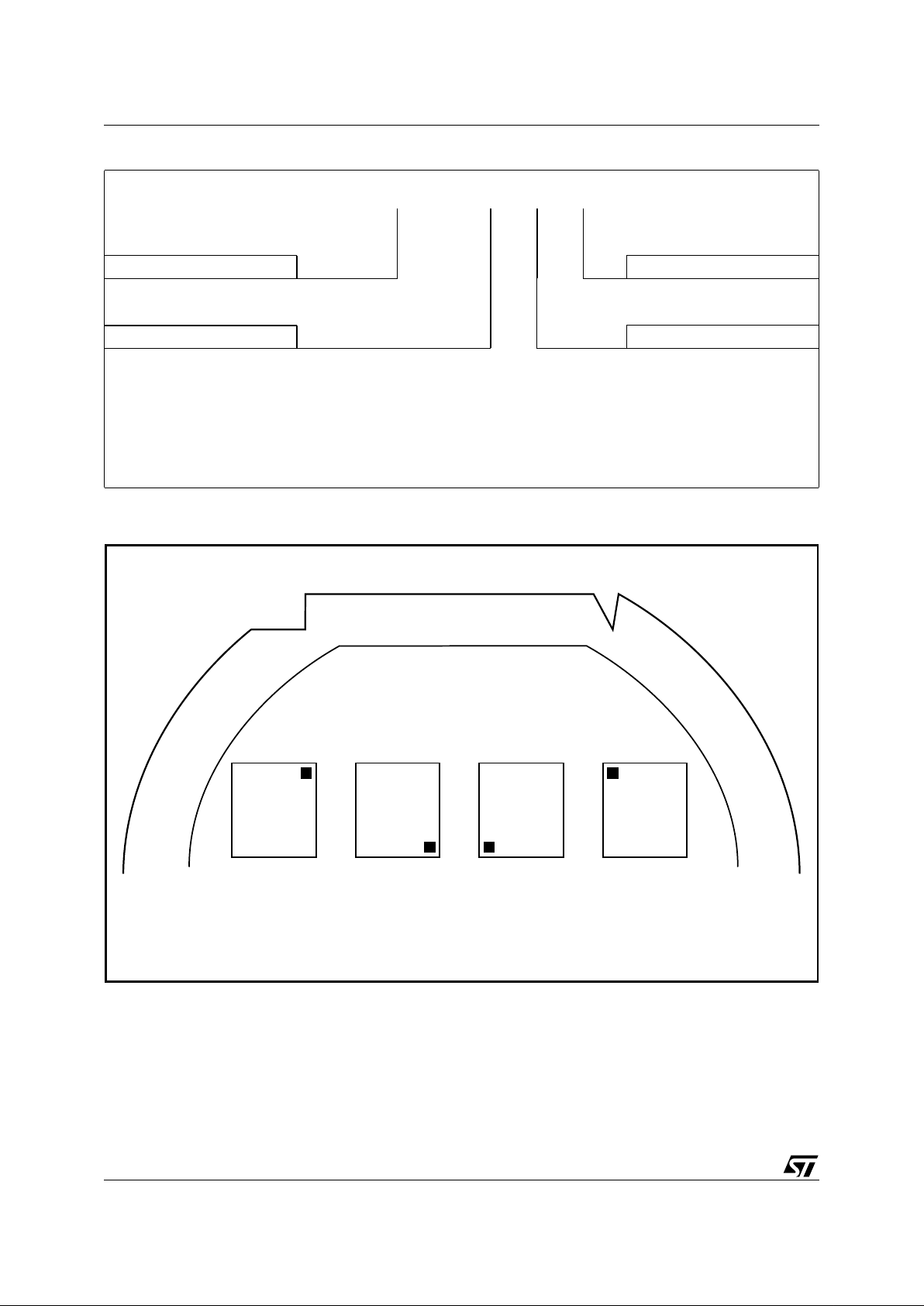
Table 4. Ordering Information Scheme
Note: *wher e “y ” i nd i cates th e sawing ori entat i on as show n i n F i gu re 2
Figure 2. Sawing orientation
Sawn wafers are scribed an d m ount ed in a frame
on adhesive tape. The orientation is defined by the
position of the GND pad on the die, viewed with
active area of product visible, relative to the notches of the frame (as shown in Figure 2). The orientation of the die with respect t o the plastic frame
notches is specified by the Customer.
One further concern, when specify ing devices to
be delivered in this form, is that wafers mounted
on adhesive tape must be used within a limited period from the mounting date:
– two months, if wafers a re stored at 25°C, 55%
relative h umidity
– six months, if wafers are stored at 4°C, 55% rel-
ative humidity
Example: ST19SF08C D45 XXX Z
Product name Pre-personalization name
“+” if no pre-personalization
Delivery Form Customer ROM code name
Dxx: Module contact or dual
Cxx: Contactless modules
Oxx: SO package
Wxx: Unsawn wafer
Sxy*: Sawn wafer (std UV tape)
Rxy*: Sawn wafer (insolated UV tape) or SO on tape and reel
AI02171
1ORIENTATION
GND
GND GND
GND
234
VIEW: WAFER FRONT SIDE
 Loading...