®
LOW CAPACITANCE DETECTION DIODE
MAIN PRODUCT CHARACTERISTICS
STDD15 series
I
F(AV)
V
RRM
10 mA
15 V
Tj (max) 150 °C
(max) 0.51 V
V
F
FEATURES AND BENEFITS
Low diode capacitance
■
Device designed for RF application
■
Low profile package
■
Available in 3 configurations
■
■ Very low parasitic inductor & resistor
DESCRIPTION
The STDD15 is a dual diode series for the
detection of a RF signal and the compensation of
thevoltagedriftwiththe temperature. TheSOT323
package makes the device ideal in application
where the space saving is critical like mobile
phones.
The low junction capacitance will reduce the
disturbance on the RF signal
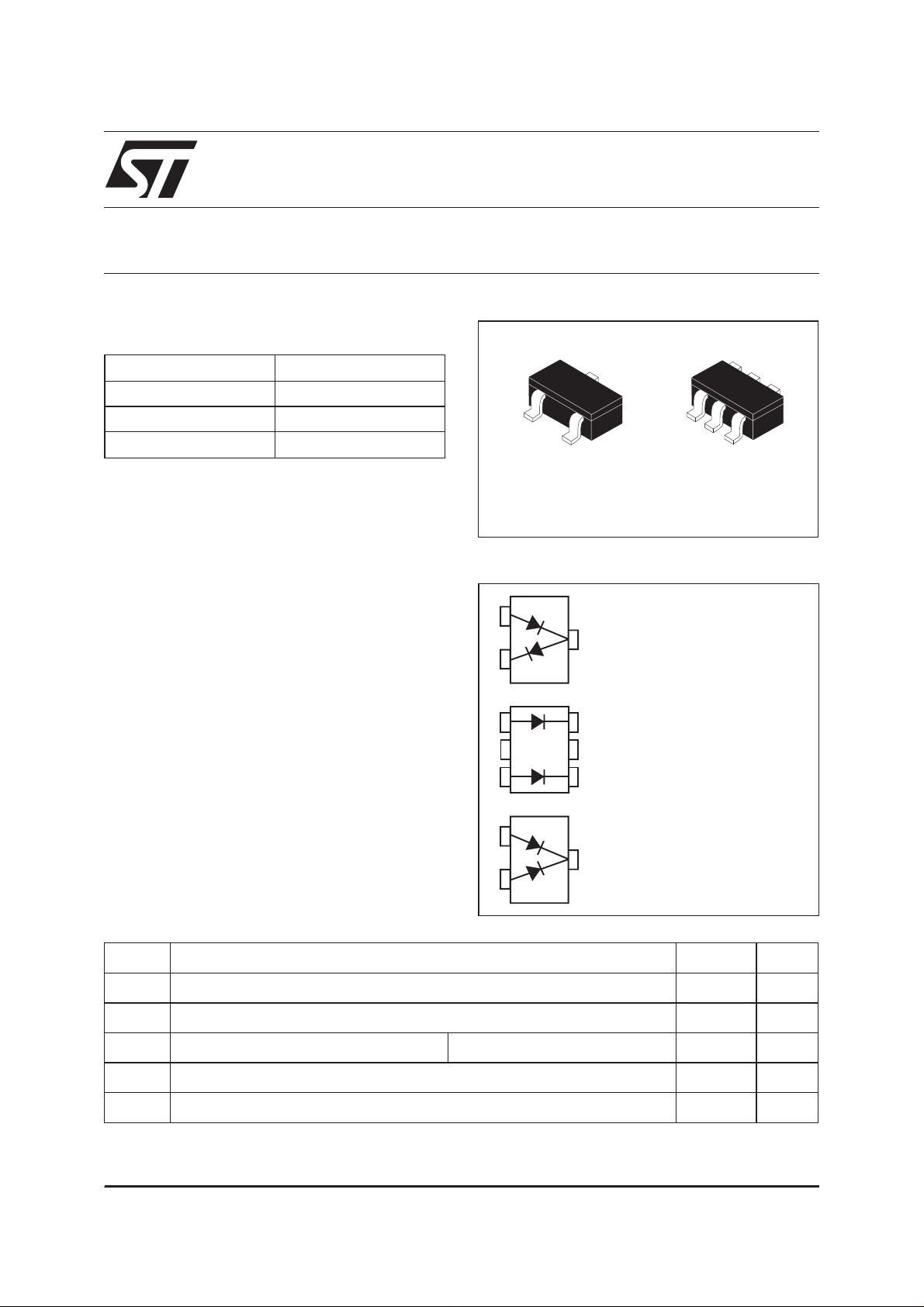
SOT323-3L
STDD15-xxW
SCHEMATIC DIAGRAM
1
3
2
1
2
3
4
5
6
SOT323-6L
STDD15-xxS
Series configuration
STDD15-04W
Parallel configuration
STDD15-07S
1
3
2
Common cathode configuration
STDD15-05W
ABSOLUTE RATINGS (limiting values)
Symbol Parameter Value Unit
V
RRM
I
FSM
T
I
stg
Repetitive peak reverse voltage 15 V
Continuous forward current 10 mA
F
Surge non repetitive forward current tp = 10ms 2 A
Storage temperature range - 65 + 150 °C
Tj Maximum operating junction temperature 150 °C
August 2002 - Ed: 3A
1/6

STDD15 series
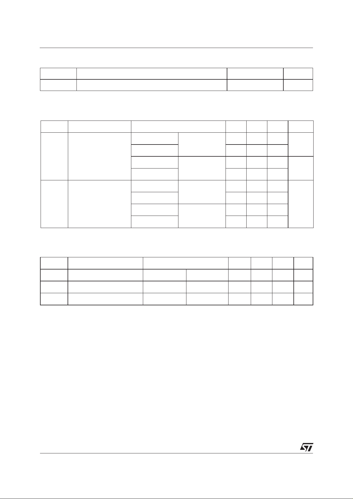
THERMAL PARAMETERS
Symbol Parameter Value Unit
R
* Junctionto ambient 500 °C/W
th (j-a)
*: Mounted with minimum recommended pad size, PC board FR4.
STATIC ELECTRICAL CHARACTERISTICS
Symbol Parameter Tests conditions Min. Typ. Max. Unit
I
* Reverse leakage
R
current
Tj = 25°C V
= 1V 0.035 µA
R
Tj = 125°C 6 30
Tj = 25°C V
= 15V 0.23 µA
R
Tj = 125°C 10 100
V
* Forward voltage drop Tj = 25°C I
F
= 1 mA 350 380 mV
F
Tj = 125°C 230 260
Tj = 25°C I
= 10 mA 500 570
F
Tj = 125°C 450 510
* Pulse test: tp ≤ 250µs, Delta ≤ 2%
ELECTRICAL CHARACTERISTICS
Symbol Parameter Tests conditions Min. Typ. Max. Unit
C Diode capacitance V
R
F
Forward resistance IF= 5 mA F = 100MHz 15 Ω
= 0 V F = 1MHz 1.0 pF
R
Ls Series inductance 1.5 nH
2/7
 Loading...