

STD60NF3LL
N-CHANNEL 30V - 0.0075Ω - 60A DPAK
STripFET™ II POWER MOSFET
TYPE V
STD60NF3LL 30V <0.0095Ω 60A
■ TYPICAL R
■ OPTIMAL RDS(O N) x Qg TRA D E-OFF @ 4.5V
■ CONDUCTION LOSSES REDUCED
■ SWITCHING LOSSES REDUCED
■ ADD SUFFIX “T4” FOR ORDERING IN TAPE &
DS
DSS
(on) = 0.0075Ω
R
DS(on)
I
D
REEL
DESCRIPTION
This application specific Powe r M osfet i s the t hird
genaration of STMicroelectronics unique “Single
Feature Size
™” strip-based process. The resul t-
ing transistor shows the best trade-off between onresistance ang gate charge. When used as high
and low side in buck regulators, it gives the best
performance in terms of both conduction and
switching losses. This is e xtremely important for
motherboards where fast switching and high e fficiency are of paramount importance.
APPLICATIONS
■ SPECIFICALLY D ESIGNED AND OP TIMISED
FOR HIGH EFFICIENCY DC/DC
CONVERTERS
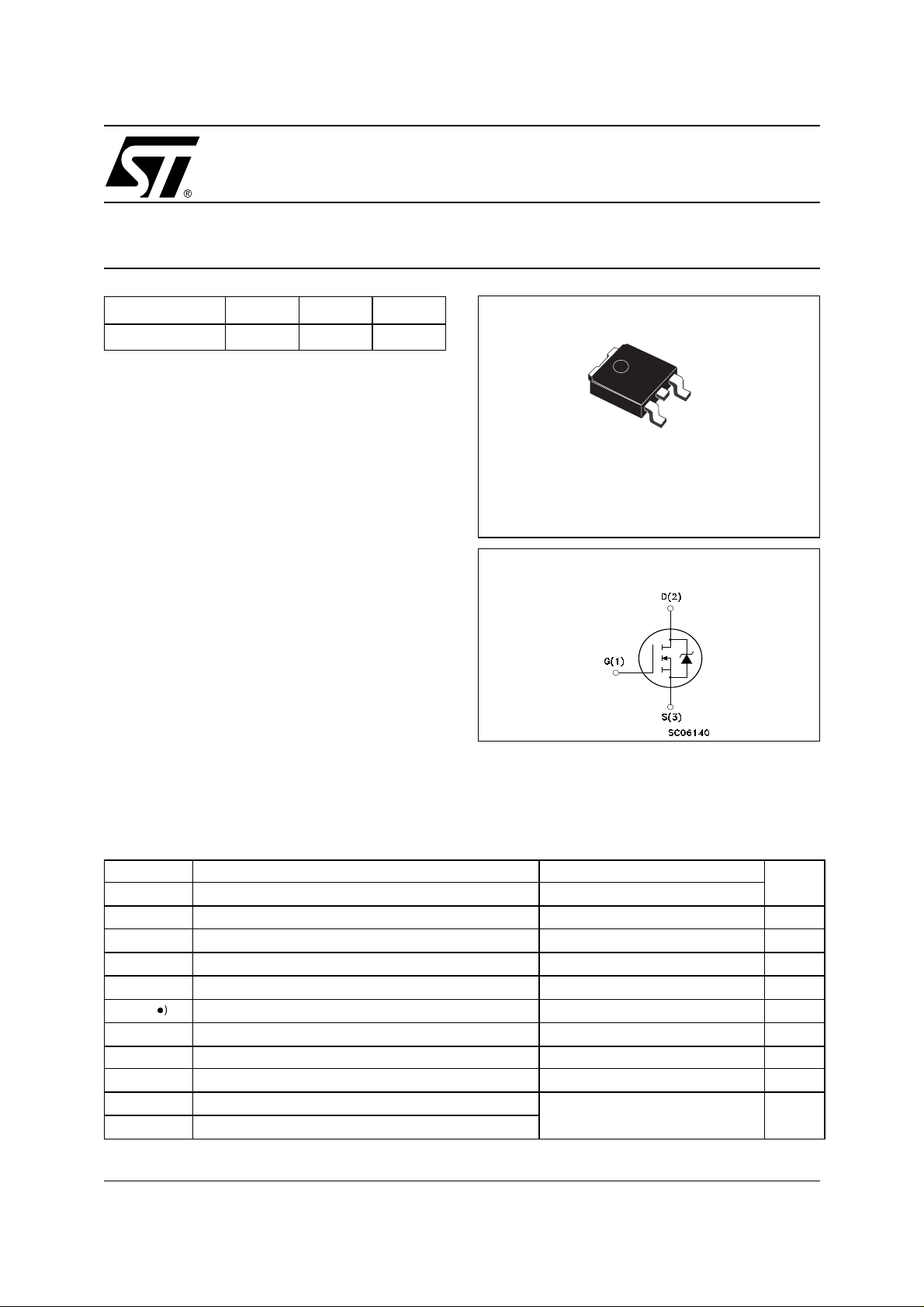
3
1
DPAK
TO-252
INTERNAL SCHEMATIC DIAGRAM
ABSOLUTE MAXIMUM RATINGS
Symbol Parameter Value Unit
V
DS
V
DGR
V
GS
I
D
I
D
I
DM
P
TOT
E
AS
T
stg
T
j
(●) Pulse width limited by safe operating area
Drain-source Voltage (VGS = 0)
Drain-gate Voltage (RGS = 20 kΩ)
Gate- source Voltage ± 16 V
Drain Current (continuos) at TC = 25°C
Drain Current (continuos) at TC = 100°C
(l)
Drain Current (pulsed) 240 A
Total Dissipation at TC = 25°C
Derating Factor 0.67 W/°C
(1)
Single Pulse Avalanche Energy 700 mJ
Storage Temperature
Operating Junction Temperature
(1) Starting Tj=25°C, ID=30A, VDD=27.5V
30 V
30 V
60 A
43 A
100 W
– 55 to 175 °C
1/9April 2002
STD60NF3LL
THERMA L D ATA
Rthj-case Thermal Resistance Junction-case Max 1.5 °C/W
Rthj-amb Thermal Resistance Junction-ambient Max 100 °C/W
T
l
ELECTRICAL CHARACTERISTICS (TCASE = 25 °C UNLESS OTHERWISE SPECIFIED)
OFF
Symbol Parameter Test Conditions Min. Typ. Max. Unit
V
(BR)DSS
I
DSS
I
GSS
ON
(1)
Symbol Parameter Test Conditions Min. Typ. Max. Unit
V
GS(th)
R
DS(on)
Maximum Lead Temperature For Soldering Purpose 300 °C
Drain-source
ID = 250 µA, VGS = 0 30 V
Breakdown Voltage
Zero Gate Voltage
Drain Current (V
GS
= 0)
Gate-body Leakage
Current (V
DS
= 0)
Gate Threshold Voltage
Static Drain-source On
Resistance
V
= Max Rating
DS
V
= Max Rating, TC = 125 °C
DS
V
= ± 16V ±100 nA
GS
V
= VGS, ID = 250µA
DS
= 10 V, ID = 30 A
V
GS
VGS = 4.5 V , ID = 30 A
1V
0.0075
0.0085
1µA
10 µA
0.0095
0.0105
Ω
Ω
DYNAMIC
Symbol Parameter Test Conditions Min. Typ. Max. Unit
(1) Forward Transconductance VDS =15 V, ID=30 A 30 S
g
fs
C
iss
C
oss
C
rss
Input Capacitance
Output Capacitance 635 pF
Reverse Transfer
Capacitance
V
= 25V, f = 1 MHz, VGS = 0
DS
2210 pF
138 pF
2/9
STD60NF3LL
ELECTRICAL CHARACTERISTICS (CONTINUED)
SWITCHING ON
Symbol Parameter Test Conditions Min. Typ. Max. Unit
V
t
d(on)
Q
Q
Q
t
r
g
gs
gd
Turn-on Delay Time
Rise Time 130 ns
Total Gate Charge
Gate-Source Charge
Gate-Drain Charge
SWITCHING OFF
Symbol Parameter Test Conditions Min. Typ. Max. Unit
t
d(off)
t
d(off)
t
f
t
f
t
c
Turn-off-Delay Time
Fall Time
Off-voltage Rise Time
Fall Time
Cross-over Time
SOURCE DRAIN DIODE
Symbol Parameter Test Conditions Min. Typ. Max. Unit
I
SD
I
SDM
VSD (2)
t
rr
Q
rr
I
RRM
Note: 1. Pulsed: Pu l se duration = 300 µs, duty cyc l e 1.5 %.
2. Pulse width li mited by safe operating ar ea.
Source-drain Current 60 A
(1)
Source-drain Current (pulsed) 240 A
Forward On Voltage
Reverse Recovery Time
Reverse Recovery Charge
Reverse Recovery Current
= 15V, ID = 30A
DD
R
= 4.7Ω VGS = 4.5V
G
(see test circuit, Figure 3)
= 24V, ID = 60A,
V
DD
VGS = 4.5V
= 15V, ID = 30A,
V
DD
RG=4.7Ω, V
GS
= 4.5V
(see test circuit, Figure 3)
GS
=30A
D
= 4.5V
Vclamp =24V, I
R
=4.7Ω, V
G
(see test circuit, Figure 5)
ISD = 60A, VGS = 0
= 60A, di/dt = 100A/µs,
I
SD
VDD = 15V, Tj = 150°C
(see test circuit, Figure 5)
22 ns
30
40 nC
9
12.5
36.5
36.5
32
23
40
1.2 V
65
105
3.4
nC
nC
ns
ns
ns
ns
ns
ns
nC
A
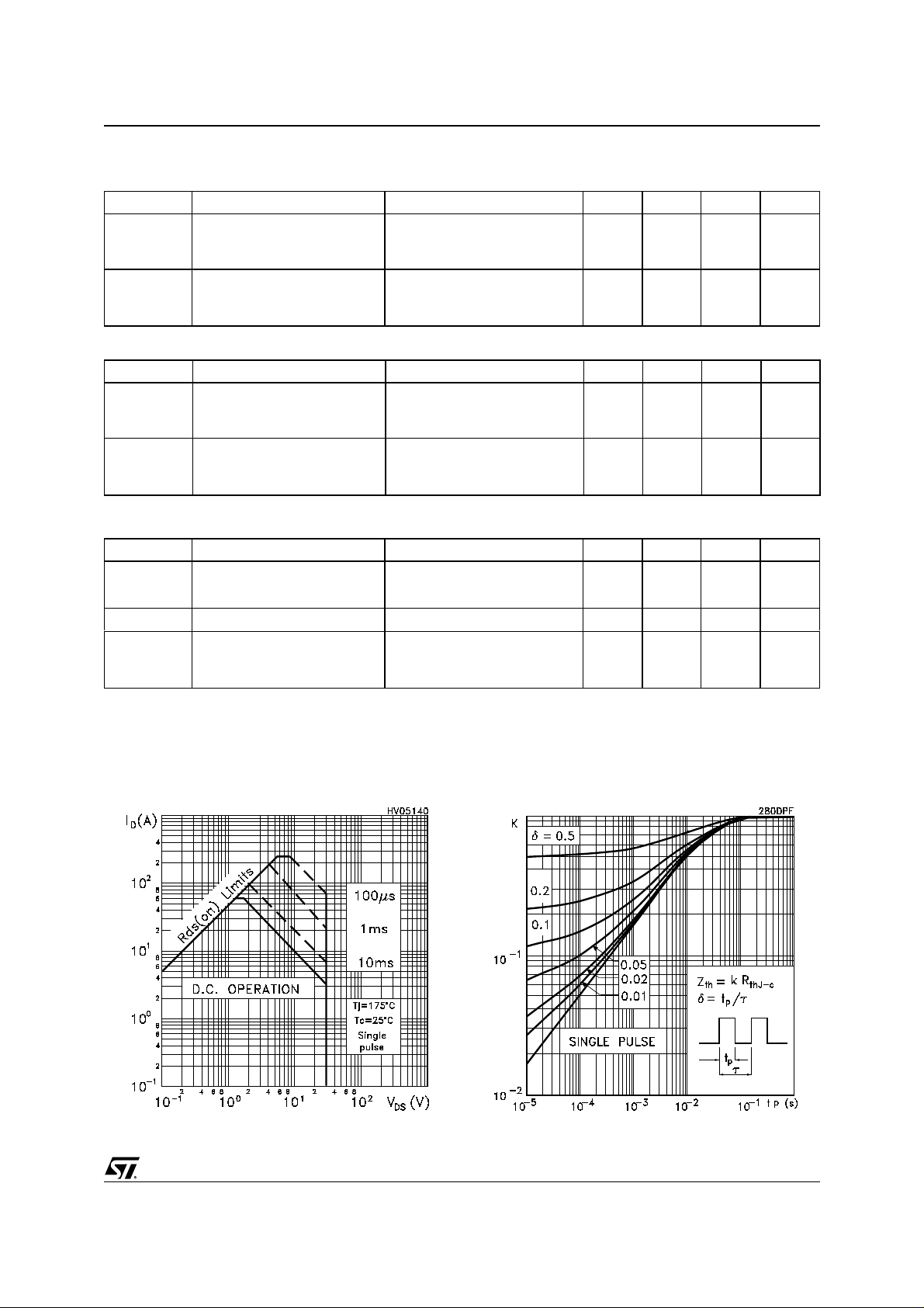
Thermal ImpedenceSafe Operating Area
3/9
 Loading...