

1/8May 2000
STD5NM50
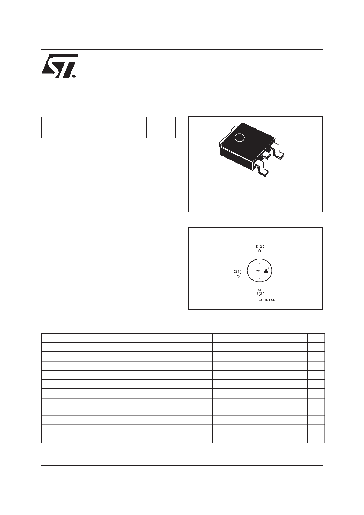
N-CHANNEL 500V - 0.7Ω - 5A DPAK
MDmeshPower MOSFET
■ TYPICAL R
DS
(on) = 0.7Ω
■ HIGH dv/dt AND AVALANCHE CAPABILITIES
■ 100% AVALANCHE TESTED
■ LOW INPUT CAPACITANCE AND GATE
CHARGE
■ LOW GATE INPUT RESISTANCE
■ TIGHT PROCESS CONTROL AND HIGH
MANUFACTURING YIELDS
DESCRIPTION
The MDmesh is a new revolutionary MOSFET
technology that associates the Multiple Drain process with the Company’s PowerMESH horizontal
layout. The resulting producthasanoutstanding low
on-resistance, impressively high dv/dtand excellent
avalanche characteristics. The adoption of the
Company’s proprietary strip technique yields overall
dynamic performancethat issignificantly better than
that of similar competition’s products.
APPLICATIONS
The MDmesh family isverysuitableforincreasing
power density of high voltage converters allowing
system miniaturization and higher efficiencies.
ABSOLUTE MAXIMUM RATINGS
(•)Pulse width limitedby safe operating area
TYPE V
DSS
R
DS(on)
I
D
STD5NM50 500V <0.8Ω 5A
Symbol Parameter Value Unit
V
DS
Drain-source Voltage (VGS= 0) 500 V
V
DGR
Drain-gate Voltage (RGS=20kΩ) 500 V
V
GS
Gate- source Voltage ±30 V
I
D
Drain Current (continuos) at TC=25°C5A
I
D
Drain Current (continuos) at TC= 100°C 3.1 A
I
DM
(●) Drain Current (pulsed) 20 A
P
TOT
TotalDissipation at TC=25°C
50 W
Derating Factor 0.4 W/°C
dv/dt Peak Diode Recovery voltage slope 6 V/ns
T
stg
Storage Temperature –65 to 150 °C
T
j
Max. Operating Junction Temperature 150 °C
1
3
DPAK
TO-252
INTERNAL SCHEMATIC DIAGRAM
STD5NM50
2/8
THERMAL DATA
AVALANCHE CHARACTERISTICS
ELECTRICAL CHARACTERISTICS (TCASE = 25 °C UNLESS OTHERWISE SPECIFIED)
OFF
ON (1)
DYNAMIC
Note: 1. Pulsed: Pulse duration = 300 µs, duty cycle 1.5%.
Rthj-case Thermal Resistance Junction-case Max 2.5 °C/W
Rthj-amb Thermal Resistance Junction-ambient Max 62.5 °C/W
Rthc-sink Thermal Resistance Case-sink Typ 0.5 °C/W
T
l
Maximum Lead Temperature For Soldering Purpose 300 °C
Symbol Parameter Max Value Unit
I
AR
Avalanche Current, Repetitive or Not-Repetitive
(pulse width limited by T
j
max)
5A
E
AS
Single Pulse Avalanche Energy
(starting T
j
=25°C, ID=IAR,VDD=50V)
200 mJ
Symbol Parameter Test Conditions Min. Typ. Max. Unit
V
(BR)DSS
Drain-source
Breakdown Voltage
I
D
= 250 µA, VGS=0
500 V
I
DSS
Zero Gate Voltage
Drain Current (V
GS
=0)
V
DS
= Max Rating
1 µA
V
DS
= Max Rating, TC= 125 °C
10 µA
I
GSS
Gate-body Leakage
Current (V
DS
=0)
V
GS
= ±30V
±100 nA
Symbol Parameter Test Conditions Min. Typ. Max. Unit
V
GS(th)
Gate Threshold Voltage
V
DS=VGS,ID
= 250µA
345V
R
DS(on)
Static Drain-source On
Resistance
V
GS
= 10V, ID= 2.5A
0.7 0.8 Ω
I
D(on)
On State Drain Current
V
DS>ID(on)xRDS(on)max,
VGS=10V
5A
Symbol Parameter Test Conditions Min. Typ. Max. Unit
g
fs
(1)
Forward Transconductance
V
DS>ID(on)xRDS(on)max,
ID= 2.5A
2.4 S
C
iss
Input Capacitance
V
DS
= 25V, f = 1 MHz, VGS=0
415 pF
C
oss
Output Capacitance 88 pF
C
rss
Reverse Transfer
Capacitance
12 pF
R
G
Gate Input Resistance
f=1 MHz Gate DC Bias = 0
Test Signal Level = 20mV
Open Drain
3 Ω
3/8
STD5NM50
ELECTRICAL CHARACTERISTICS (CONTINUED)
SWITCHING ON
SWITCHING OFF
SOURCE DRAIN DIODE
Note: 1. Pulsed: Pulse duration = 300 µs, duty cycle 1.5 %.
2. Pulse width limited by safe operating area.
Symbol Parameter Test Conditions Min. Typ. Max. Unit
t
d(on)
Turn-on Delay Time
V
DD
= 250V, ID= 2.5A
R
G
= 4.7Ω VGS= 10V
(see test circuit, Figure 3)
16 ns
t
r
Rise Time 8 ns
Q
g
TotalGate Charge
V
DD
= 400V, ID= 5A,
V
GS
= 10V
13 nC
Q
gs
Gate-Source Charge 4 nC
Q
gd
Gate-Drain Charge 6 nC
Symbol Parameter TestConditions Min. Typ. Max. Unit
t
r(Voff)
Off-voltage Rise Time
V
DD
= 400V, ID= 5A,
R
G
= 4.7Ω, VGS=10V
(see test circuit, Figure 5)
14 ns
t
f
Fall Time 6 ns
t
c
Cross-over Time 13 ns
Symbol Parameter Test Conditions Min. Typ. Max. Unit
I
SD
Source-drain Current 5 A
I
SDM
(2)
Source-drain Current (pulsed) 20 A
V
SD
(1)
Forward On Voltage
ISD= 5A, VGS=0
1.5 V
t
rr
Reverse Recovery Time
I
SD
= 5A, di/dt = 100A/µs,
V
DD
= 100V, Tj= 150°C
(see test circuit, Figure 5)
270 ns
Q
rr
Reverse Recovery Charge 1.6 µC
I
RRM
Reverse Recovery Current 12 A
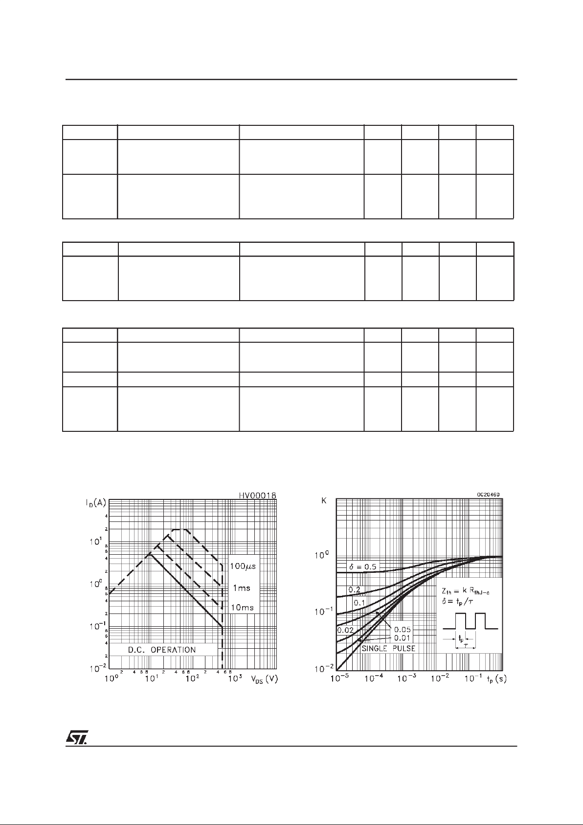
Safe Operating Area Thermal Impedance

STD5NM50
4/8
Static Drain-source On Resistance
Transfer Characteristics
Transconductance
Output Characteristics
Capacitance VariationsGate Charge vs Gate-source Voltage

5/8
STD5NM50
Normalized On Resistance vs TemperatureNormalized Gate Threshold Voltage vs
Temperature
Source-drain Diode Forward Characteristics

STD5NM50
6/8
Fig. 5: Test Circuit For Inductive Load Switching
And Diode Recovery Times
Fig. 4: Gate Charge test Circuit
Fig. 2: Unclamped Inductive WaveformFig. 1: Unclamped Inductive Load Test Circuit
Fig. 3: Switching Times Test Circuit For
Resistive Load

7/8
STD5NM50
DIM.
mm inch
MIN. TYP. MAX. MIN. TYP. MAX.
A 2.20 2.40 0.087 0.094
A1 0.90 1.10 0.035 0.043
A2 0.03 0.23 0.001 0.009
B 0.64 0.90 0.025 0.035
B2 5.20 5.40 0.204 0.213
C 0.45 0.60 0.018 0.024
C2 0.48 0.60 0.019 0.024
D 6.00 6.20 0.236 0.244
E 6.40 6.60 0.252 0.260
G 4.40 4.60 0.173 0.181
H 9.35 10.10 0.368 0.398
L2 0.8 0.031
L4 0.60 1.00 0.024 0.039
V2 0
o
8
o
0
o
0
o
P032P_B
TO-252 (DPAK) MECHANICAL DATA

STD5NM50
8/8
Information furnished isbelieved tobe accurate and reliable. However, STMicroelectronics assumes noresponsibility for theconsequences
of use of such information nor for any infringement of patents or other rights of third parties which may result from its use. No license is
granted by implication orotherwise underany patent or patent rights of STMicroelectronics. Specification mentioned in this publication are
subject tochange without notice. This publication supersedes and replaces allinformation previously supplied. STMicroelectronics products
are not authorized for useas critical components in life support devices or systems without express written approval of STMicroelectronics.
The ST logois a trademarkof STMicroelectronics
2000 STMicroelectronics – Printedin Italy– AllRights Reserved
STMicroelectronicsGROUP OF COMPANIES
Australia -Brazil -China - Finland- France- Germany- HongKong - India- Italy- Japan - Malaysia- Malta -Morocco -
Singapore - Spain -Sweden -Switzerland -United Kingdom- U.S.A.
http://www.st.com
 Loading...