

STD5NE10
N - CHANNEL 100V - 0.32 Ω - 5A TO-251/TO-252
STripFET POWER MOSFET
TYPE V
DSS
R
DS(o n)
I
D
ST D5NE10 100 V < 0.4 Ω 5A
■ TYPICALR
■ EXCEPTIONALdv/dtCAPABILITY
■ AVALANCHETESTED
■ 100%AVALANCHETESTED
■ APPLICATIONORIENTED
DS(on)
= 0.32 Ω
CHARACTERIZATION
■ ADDSUFFIX ”T4” FORORDERING IN TAPE
& REEL
DESCRIPTION
This Power MOSFET is the latest developmentof
STMicroelectronics unique ”Single Feature
Size” strip-based process. The resulting transi-
stor shows extremelyhigh packing density forlow
on-resistance, rugged avalanche characteristics
and less critical alignment steps therefore a remarkablemanufacturingreproducibility.
APPLICATIONS
■ MOTORCONTROL (DISKDRIVES, etc.)
■ DC-DC& DC-AC CONVERTERS
■ SYNCHRONOUSRECTIFICATION
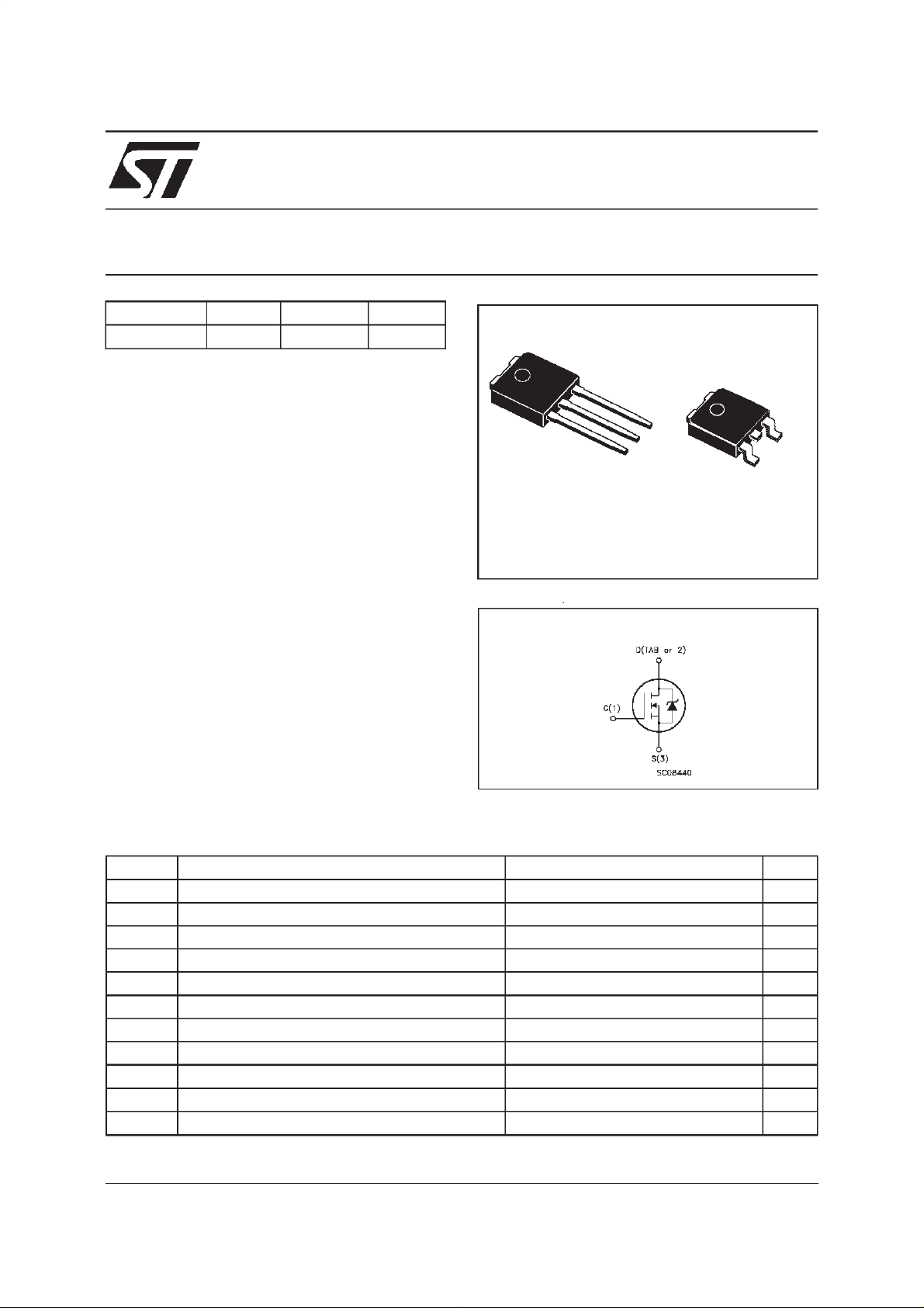
3
2
IPAK
TO-251
(Suffix”-1”)
1
(Suffix”T4”)
1
DPAK
TO-252
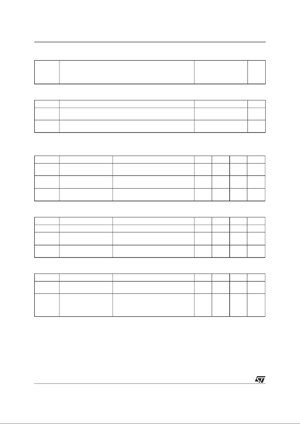
INTERNAL SCHEMATIC DIAGRAM
3
ABSOLUTE MAXIMUM RATINGS
Symbol Parameter Value Uni t
V
V
V
I
DM
P
dv/ dt (
T
(•) Pulse width limited by safe operating area (1)ISD≤ 5A, di/dt ≤ 200 A/µs,VDD≤ V
May 1999
Drain-source Voltage (VGS= 0) 100 V
DS
Drain- g at e Voltage (RGS=20kΩ) 100 V
DGR
Gate-source Voltage ± 20 V
GS
I
Drain Cur rent (c ont in uous ) at Tc=25oC5A
D
I
Drain Cur rent (c ont in uous ) at Tc=100oC3.5A
D
(•) Drain Current (pulsed) 20 A
Total Dissipation at Tc=25oC25W
tot
Derat ing F ac tor 0.17 W/
1 ) Peak Diode Recov ery volt a ge slope 0.6 V/ ns
Sto rage Temperat ure -65 to 175
stg
T
Max. Operating Junct ion Tempe r at ure 175
j
,Tj≤T
(BR)DSS
JMAX
o
C
o
C
o
C
1/9
STD5NE10
THERMAL DATA
R
thj-case
R
thj-amb
R
thc-sink
T
AVALANCHE CHARACTERISTICS
Symbol Parameter Max Value Unit
I
AR
E
Ther mal Resistanc e Junct ion-case Max
Ther mal Resistanc e Junct ion-ambient Max
Ther mal Resistanc e Case-sink Ty p
Maximum Lead Temperatu re For Soldering Purpos e
l
Avalanche C urrent, Repetitive or Not-Repetitive
(pulse width limited by T
Single Pul se Avalanc he Ener gy
AS
(starting T
=25oC, ID=IAR,VDD=30V)
j
max)
j
6
100
1.5
275
5A
25 mJ
o
C/W
o
C/W
o
C/W
o
C
ELECTRICAL CHARACTERISTICS
=25oC unless otherwisespecified)
(T
case
OFF
Symbol Parameter Test Condit ions Min. Typ. Max. Unit
V
(BR)DSS
Drain-source
ID=250µAVGS= 0 100 V
Break dow n Vo lt age
I
DSS
I
GSS
Zero Gate Voltage
Drain Curre nt (V
GS
Gat e- bod y Leakag e
Current (V
DS
=0)
=0)
V
=MaxRating
DS
=MaxRating Tc= 125oC
V
DS
V
=± 20 V
GS
1
10
100 nA
±
ON(∗)
Symbol Parameter Test Condit ions Min. Typ. Max. Unit
V
GS(th)
R
DS(on)
Gate Threshold Voltage VDS=VGSID= 250 µA 234V
Sta t ic Drain-s our c e On
VGS=10V ID= 2.5 A 0.32 0.4
Resistance
I
D(on)
On State Drain Current VDS>I
D(on)xRDS(on )max
5A
VGS=10V
DYNAMIC
Symbol Parameter Test Condit ions Min. Typ. Max. Unit
g
(∗)Forward
fs
Tr ansc on duc tance
C
C
C
Input Capaci t ance
iss
Out put Capac itance
oss
Reverse Transfer
rss
Capacit a nc e
VDS>I
D(on)xRDS(on )maxID
=2.5A 2.5 S
VDS=25V f=1MHz VGS= 0 305
45
21
µ
µA
Ω
pF
pF
pF
A
2/9

STD5NE10
ELECTRICAL CHARACTERISTICS
(continued)
SWITCHINGON
Symbol Parameter Test Condit ions Min. Typ. Max. Unit
t
d(on)
Tur n-on Delay Time
Rise Time
t
r
VDD=50V ID=3.5A
R
=4.7
G
Ω
VGS=10V
6.5
15
(Resis t iv e Load, see fig. 3)
Q
Q
Q
Tot al Gate Charge
g
Gat e- Source Charge
gs
Gate-Drain Charge
gd
VDD=80V ID=5A VGS=10V 14
6
4
18 nC
SWITCHINGOFF
Symbol Parameter Test Condit ions Min. Typ. Max. Unit
t
d(off)
Tur n-of f Dela y Tim e
t
Fall T ime
f
VDD=50V ID=3.5A
=4.7 Ω VGS=10V
R
G
25
7
(Resis t iv e Load, see fig. 3)
t
r(Voff)
t
t
Off-volt age Rise Time
Fall T ime
f
Cross-over Tim e
c
VDD=80V ID=7A
=4.7 Ω VGS=10V
R
G
(Indu ct iv e Load, see fig. 5)
7
8
16
SOURCEDRAINDIODE
Symbol Parameter Test Condit ions Min. Typ. Max. Unit
I
SD
I
SDM
V
SD
t
Q
I
RRM
(∗) Pulsed: Pulse duration = 300 µs, duty cycle 1.5 %
(•) Pulse width limited by safe operating area
Source-drain Current
(•)
Source-drain Current
5
20
(pulsed)
(∗)ForwardOnVoltage ISD=8A VGS=0 1.5 V
Reverse Recovery
rr
Time
Reverse Recovery
rr
ISD=5A di/dt=100A/µs
=50V Tj=150oC
V
DD
(see test circuit, fig. 5)
75
210
Charge
Reverse Recovery
5.5
Current
ns
ns
nC
nC
ns
ns
ns
ns
ns
A
A
ns
nC
A
SafeOperating Area for Thermal Impedance
3/9
 Loading...