

SGS Thomson Microelectronics STP4NK50ZFP, STP4NK50Z, STD4NK50Z-1, STD4NK50Z Datasheet
STP4NK50Z - STP4NK50ZFP
STD4NK50Z - STD4NK50Z-1
N-CHANNEL 500V - 2.4Ω - 3A TO-220/TO-220FP/DPAK/IPAK
Zener-Protected SuperMESH™Power MOSFET
TYPE V
STP4NK50Z
STP4NK50ZFP
STD4NK50Z
STD4NK50Z-1
■ TYPICAL R
■ EXTREMELY HIGH dv/dtCAPABILITY
■ 100% AVALANCHE TESTED
■ GAT E CHARGE MINIMIZED
■ VERY LOW INTRINSIC CAPACITANCES
■ VER Y GOOD MANUFACTURING
500 V
500 V
500 V
500 V
(on) = 2.3 Ω
DS
DSS
R
DS(on)
< 2.7 Ω
< 2.7 Ω
< 2.7 Ω
< 2.7 Ω
I
D
3A
3A
3A
3A
Pw
45 W
20 W
45 W
45 W
REPEATIBILITY
DESCRIPTION
The SuperMESH ™ series is obtained through an
extreme optimi za tio n of ST’s well established stripbased PowerMESH™ layout. In addition to pushing
on-resistance significantly down, special care is taken to ensure a very good dv/dt capability for the
most demanding applications. Such series complements ST full range of high voltage MOSFETs i ncluding revolutionary MDmesh™ products.
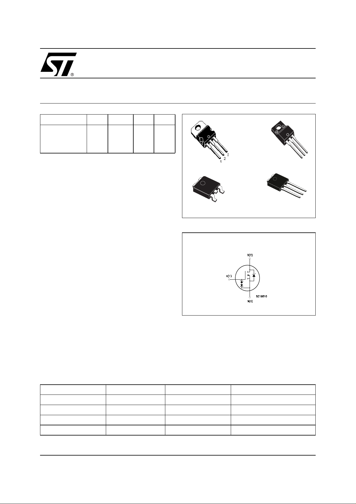
TO-220 TO-220FP
3
1
DPAK
IPAK
INTERNAL SCHEMATIC DIAGRAM
3
2
1
3
2
1
APPLICATIONS
■ HIGH CURRENT, HIGH SPEED SWITCHING
■ IDEAL FOR OFF-LINE POWER SUPPLIES,
ADAPTORS AND PFC
■ LI GHTING
ORDERING INFORMATION
SALES TYPE MARKING PACKAGE PACKAGING
STP4NK50Z P4NK50Z TO-220 TUBE
STP4NK50ZFP P4NK50ZFP TO-220FP TUBE
STD4NK50ZT4 D4NK50Z DPAK TAPE & REEL
STD4NK50Z-1 D4NK50Z IPAK TUBE
1/13December 2002
STP4NK50Z - STP4NK50ZFP - S TD4N K 50Z - STD4NK50Z-1
ABSOLUTE MAXIMUM RATINGS
Symbol Parameter Value Unit
STP4NK50Z STP4NK50ZFP
I
V
DM
P
V
DGR
V
I
I
TOT
DS
GS
D
D
Drain-source Voltage (VGS=0)
Drain-gate Voltage (RGS=20kΩ)
500 V
500 V
Gate- source Voltage ± 30 V
Drain Current (continuous) at TC= 25°C
Drain Current (continuous) at TC= 100°C
()
Drain Current (pulsed) 12 12 (*) 12 (*) A
Total Dissipation at TC= 25°C
3 3 (*) 3 (*) A
1.9 1.9 (*) 1.9 (*) A
45 20 45 W
Derating Factor 0.36 0.16 0.36 W/°C
V
ESD(G-S)
Gate source ESD(HBM-C=100pF, R=1.5KΩ) 2800 V
dv/dt (1) Peak Diode Recovery voltage slope 4.5 V/ns
V
ISO
T
j
T
stg
() Pulse width limited by safe operating area
≤3A,di/dt≤200A/µs, VDD≤ V
(1) I
SD
(*) Limited only by maximum temperature allowed
Insulation Withstand Voltage (DC) - 2500 - V
Operating Junction Temperature
Storage Temperature
(BR)DSS,Tj≤TJMAX.
-55to150 °C
STD4NK50Z
STD4NK50Z-1
THERMAL DATA
TO-220 TO-220FP
Rthj-case Thermal Resistance Junction-case (Max) 2.78 6.25 2.78 °C/W
Rthj-amb Thermal Resistance Junction-ambient (Max) 62.5 100 °C/W
T
l
Maximum Lead Temperature For Soldering Purpose
300 °C
DPAK
IPAK
AVALANCHE CHARACTERISTICS
Symbol Parameter Max Value Unit
I
AR
Avalanche Current, Repetitive or Not-Repetitive
(pulse width limited by T
E
AS
Single Pulse Avalanche Energy
(starting T
max)
j
= 25 °C, ID=IAR,VDD=50V)
j
3A
120 mJ
GATE-SOURCE ZENER DIODE
Symbol Parameter Test Conditions Min. Typ. Max. Unit
BV
GSO
Gate-Source Breakdown
Igs=± 1mA (Open Drain) 30 V
Voltage
PROTECTION FEATURES OF GATE-TO-SOURCE ZENER DIOD ES
The built-in back-to-back Zener diodes have specifically been designed to enhance not only the device’s
ESD capability, but also to make them safely absorb possibl e voltage transients that may occasionally be
applied from gate to source. In this r es pect the Zener voltage is appropriate to achieve an efficient and
cost-effective intervention to protect the device’s integrity. These integrated Zener diodes thus avoid the
usage of external components.
2/13
STP4NK50Z - STP4NK50ZFP - STD4NK50Z - STD4NK50Z-1
ELECTRICAL CHARACTERISTICS (T
=25°C UNLESS OTHERWISE SPECIFIED)
CASE
ON/OFF
Symbol Parameter Test Conditions Min. Typ. Max. Unit
V
(BR)DSS
Drain-source
ID=1mA,VGS= 0 500 V
Breakdown Voltage
I
DSS
I
GSS
V
GS(th)
R
DS(on)
Zero Gate Voltage
Drain Current (V
GS
=0)
Gate-body Leakage
Current (V
DS
=0)
Gate Threshold Voltage
Static Drain-source On
V
= Max Rating
DS
VDS= Max Rating, TC= 125 °C
V
= ± 20V ±10 µA
GS
V
DS=VGS,ID
= 50µA
3 3.75 4.5 V
1
50
VGS=10V,ID= 1.5 A 2.3 2.7 Ω
Resistance
DYNAMIC
Symbol Parameter Test Conditions Min. Typ. Max. Unit
(1) Forward Transconductance VDS=15V,ID= 1.5 A 1.5 S
g
fs
C
oss eq.
C
iss
C
oss
C
rss
Input Capacitance
Output Capacitance
Reverse Transfer
Capacitance
(3) Equivalent Output
=25V,f=1MHz,VGS= 0 310
V
DS
49
10
VGS=0V,VDS= 0V to 400V 33 pF
Capacitance
SWITCHING ON
Symbol Parameter Test Conditions Min. Typ. Max. Unit
t
d(on)
Q
Q
Q
Turn-on Delay Time
t
r
g
gs
gd
Rise Time
Total Gate Charge
Gate-Source Charge
Gate-Drain Charge
VDD=250V,ID= 1.5 A
RG= 4.7Ω VGS=10V
(Resistive Load see, Figure 3)
=400V,ID=3A,
V
DD
V
=10V
GS
10
7
12
3
7
µA
µA
pF
pF
pF
ns
ns
nC
nC
nC
SWITCHING OFF
Symbol Parameter Test Conditions Min. Typ. Max. Unit
t
d(off)
Turn-off Delay Time
t
f
Fall Time
VDD= 250 V, ID= 1.5 A
R
=4.7ΩVGS=10V
G
21
11
(Resistive Load see, Figure 3)
t
r(Voff)
t
= 400V, ID=3A,
t
f
c
Fall Time
Cross-over Time
Off-voltage Rise Time
V
DD
RG=4.7Ω, VGS= 10V
(Inductive Load see, Figure 5)
10
10
17
SOURCE DRAIN DIODE
Symbol Parameter Test Conditions Min. Typ. Max. Unit
I
SD
I
SDM
VSD(1)
t
rr
Q
rr
I
RRM
Note: 1. Pulsed: Pulse duration = 300 µs, duty cycle 1.5 %.
2. Pulse width limited by safe operating area.
3. C
Source-drain Current
(2)
Source-drain Current (pulsed)
Forward On Voltage
Reverse Recovery Time
Reverse Recovery Charge
Reverse Recovery Current
is defined as a constant equivalent capacitance giving the same charging time as C
oss eq.
.
V
DSS
ISD= 3 A, VGS=0
I
SD
VDD=40V,Tj= 150°C
(see test circuit, Figure 5)
= 3 A, di/dt = 100A/µs
260
935
7.2
when VDSincreases from 0 to 80%
oss
3
12
1.6 V
ns
ns
ns
ns
ns
A
A
ns
nC
A
3/13
STP4NK50Z - STP4NK50ZFP - S TD4N K 50Z - STD4NK50Z-1
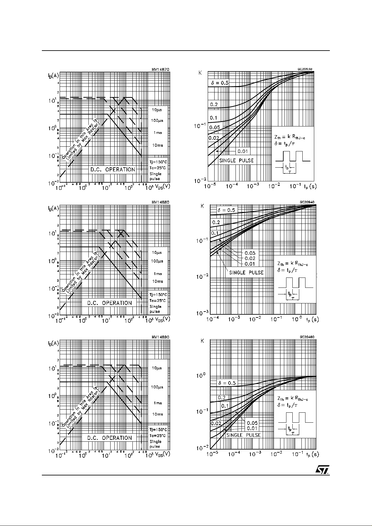
Safe Operating For TO-220
Safe Operating Area For TO-220FP Thermal Im pedance For TO-220FP
Thermal Impedance For TO-220
Safe Operating A rea For DPAK/IPAK
4/13
Thermal Impedance For DPAK/IPAK
 Loading...