

SGS Thomson Microelectronics STD4NB40 Datasheet
STD4NB40
N - CHANNEL ENHANCEMENT MODE
PowerMESH MOSFET
PRELIMINARY DATA
TYPE V
DSS
R
DS(on)
I
D
ST D4 NB40 400 V < 1.8 Ω 3.7 A
■ TYPICALR
■ EXTREMELY HIGH dv/dt CAPABILITY
■ 100% AVALANCHETESTED
■ VERYLOW INTRINSIC CAPACITANCES
■ GATECHARGEMINIMIZED
DS(on)
=1.47 Ω
DESCRIPTION
Using the latest high voltage MESH OVERLAY
process, SGS-Thomson has designed an
advanced family of power MOSFETs with
outstanding performances. The new patent
pending strip layout coupled with the Company’s
proprietary edge termination structure, gives the
lowest R
per area, exceptional avalanche
DS(on)
and dv/dt capabilities and unrivalled gate charge
and switching characteristics.
APPLICATIONS
■ SWITCHMODEPOWER SUPPLIES(SMPS)
■ DC-ACCONVERTERS FOR WELDING
EQUIPMENTAND UNINTERRUPTIBLE
POWERSUPPLIESAND MOTORDRIVE
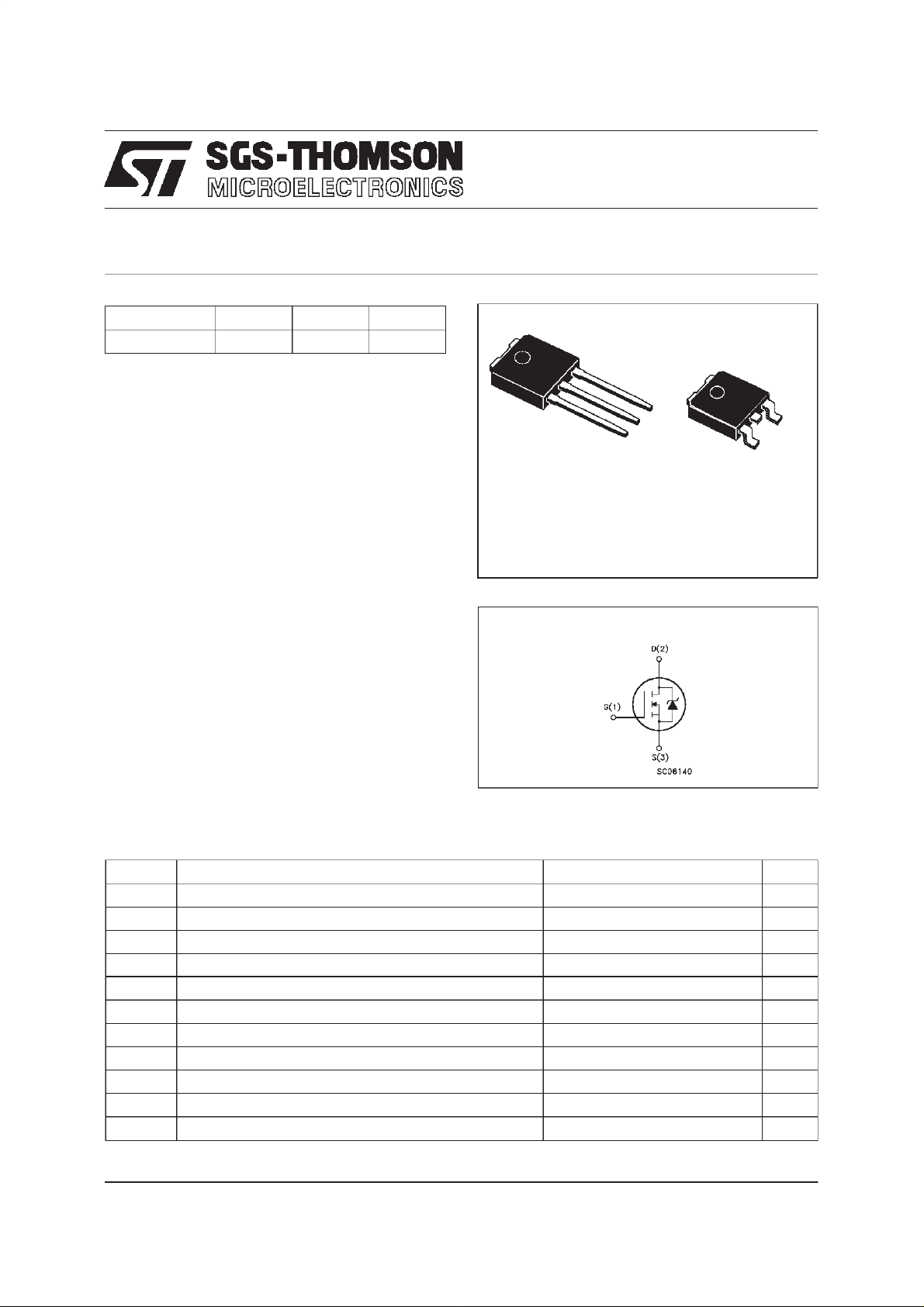
3
2
IPAK
TO-251
(Suffix”-1”)
1
(Suffix ”T4”)
1
DPAK
TO-252
INTERNAL SCHEMATIC DIAGRAM
3
ABSOLUTE MAXIMUM RATINGS
Symb o l Para meter Value Uni t
V
V
V
I
DM
P
dv/dt(
T
(•) Pulse width limited by safe operating area (1)ISD≤3.7A, di/dt ≤ 200 A/µs, VDD≤ V
February 1998
Drain-source Voltage (VGS=0) 400 V
DS
Drain- gate Voltage (RGS=20kΩ)
DGR
Gat e- source Vo lt age ± 30 V
GS
I
Drain Cur rent (c on t inuous) a t Tc=25oC3.7A
D
I
Drain Cur rent (c on t inuous) a t Tc=100oC2.3A
D
400 V
(•) Dra in Curr ent (pulsed) 14.8 A
Tot al Dissip at ion at Tc=25oC50W
tot
Derating Factor 0.4 W/
1) Peak Diode Rec overy voltage slope 4.5 V/ns
Sto rage Tempe rature -65 to 150
stg
T
Max. Operating Ju nc tion T emperat ure 150
j
,Tj≤T
(BR)DSS
JMAX
o
C
o
C
o
C
1/6
STD4NB40
THERMAL DATA
R
thj-case
Rthj-a mb
R
thc-sin k
T
AVALANCHE CHARACTERISTICS
Symbol Para met e r Max Value Uni t
I
AR
E
Ther mal Resist ance Junctio n-case Max
Ther mal Resist ance Junctio n-ambient Max
Ther mal Resist ance Case-sink T y p
Maximum Lead Tem per a t u re F o r Soldering Purpos e
l
Avalanche Cur rent, Repet it i v e or Not-Re petitive
(pulse width limited by T
Single Pulse Avalanche Energy
AS
(starting T
=25oC, ID=IAR,VDD=50V)
j
max, δ <1%)
j
2.5
100
1.5
275
3.7 A
60 mJ
o
C/W
oC/W
o
C/W
o
C
ELECTRICAL CHARACTERISTICS (T
=25oC unlessotherwise specified)
case
OFF
Symbol Parameter Test Cond itions Min. Typ. Ma x. Unit
V
(BR)DSS
Drain-sourc e
=250µAVGS=0
I
D
400 V
Breakdown V oltage
I
DSS
I
GSS
Zer o Gat e V o lt age
Drain Current (V
GS
Gat e-body Leaka ge
Current (V
DS
=0)
=0)
=MaxRating
V
DS
V
=MaxRating Tc=125oC
DS
= ± 30 V
V
GS
1
50
± 100 nA
ON (∗)
Symbol Parameter Test Cond itions Min. Typ. Ma x. Unit
V
GS(th )
Gate Threshold
V
DS=VGSID
=250µA
345V
Voltage
R
DS(on)
Stati c D rain-source On
VGS=10V ID=2.3 A 1.47 1.8 Ω
Resistance
I
D(on)
On State Drain Curre nt VDS>I
D(on)xRDS(on)max
4.7 A
VGS=10V
DYNAMIC
Symbol Parameter Test Cond itions Min. Typ. Ma x. Unit
g
(∗)Forward
fs
Tr ansconductanc e
C
C
C
Input Capac i t an c e
iss
Out put C apa c itance
oss
Reverse Transf er
rss
Capa cit an c e
VDS>I
D(on)xRDS(on)maxID
=2.3 A 1.5 2.4 S
VDS=25V f=1MHz VGS= 0 405
72
9
526
94
12
µA
µA
pF
pF
pF
2/6
STD4NB40
ELECTRICAL CHARACTERISTICS (continued)
SWITCHINGON
Symbol Parameter Test Cond itions Min. Typ. Ma x. Unit
t
d(on)
Turn-on Time
r
Rise Tim e
t
VDD=200V ID=2.3A
=4.7 Ω VGS=10V
R
G
11
8
(see test circuit, figure 3)
Q
Q
Q
Total Gate Charge
g
Gat e-Sour ce Cha rge
gs
Gate-Drain Charge
gd
VDD=320V ID=4.7 A VGS= 1 0 V 14.5
7
5.1
SWITCHINGOFF
Symbol Parameter Test Cond itions Min. Typ. Ma x. Unit
t
r(Voff)
t
t
Of f - voltage Rise Time
Fall Time
f
Cross-ov er Time
c
VDD=480V ID=4.7A
=4.7 Ω VGS=10V
R
G
(see test circuit, figure 5)
9
6
14
SOURCE DRAIN DIODE
Symbol Parameter Test Cond itions Min. Typ. Ma x. Unit
I
SD
I
SDM
V
SD
t
Q
I
RRM
(∗) Pulsed: Pulse duration =300 µs, duty cycle1.5 %
(•) Pulse width limited by safe operating area
Source-drain Curre nt
(•)
Source-drain Curre nt
(pulsed)
(∗) For ward On Volt age ISD=4.7A VGS=0 1.6 V
Reverse Recov er y
rr
Time
Reverse Recov er y
rr
= 4 .7 A di/dt = 100 A/µs
I
SD
=100V Tj=150oC
V
DD
(see test circuit, figure 5)
300
1.6
Charge
Reverse Recov er y
10.5
Current
17
12
22 nC
13
10
20
4.7
19
ns
ns
nC
nC
ns
ns
ns
A
A
ns
µC
A
3/6
 Loading...