

SGS Thomson Microelectronics STD40NF3LL Datasheet
STD40NF3LL
N-CHANNEL 30V - 0.0095
LOW GATE CHARGE STripFET POWER MOSFET
TYPE V
ST D40N F 3LL 30 V < 0.0115 Ω 40 A
■ TYPICALR
■ OPTIMAL R
■ CONDUCTION LOSSESREDUCED
■ SWITCHINGLOSSESREDUCED
DS(on)
DSS
= 0.0115 Ω @ 4.5V
DS(on)xQg
DESCRIPTION
This applicationspecific Power Mosfet is thethird
generation of STMicroelectronics unique ”Single
Feature Size” strip-based process. The resulting transistor shows the best trade-off between
on-resistance and gate charge. When used as
high and low side in buck regulators, it gives the
best performancein termsof both conductionand
switching losses. This is extremely important for
motherboardswhere fast switching and high efficiencyare of paramount importance.
APPLICATIONS
■ SPECIFICALLYDESIGNED AND
OPTIMISEDFOR HIGH EFFICIENCYCPU
CORE DC/DC CONVERTERS
R
DS(on)
I
D
TRADE-OFF@ 4.5V
Ω
- 40A DPAK
PRELIMINARY DATA
3
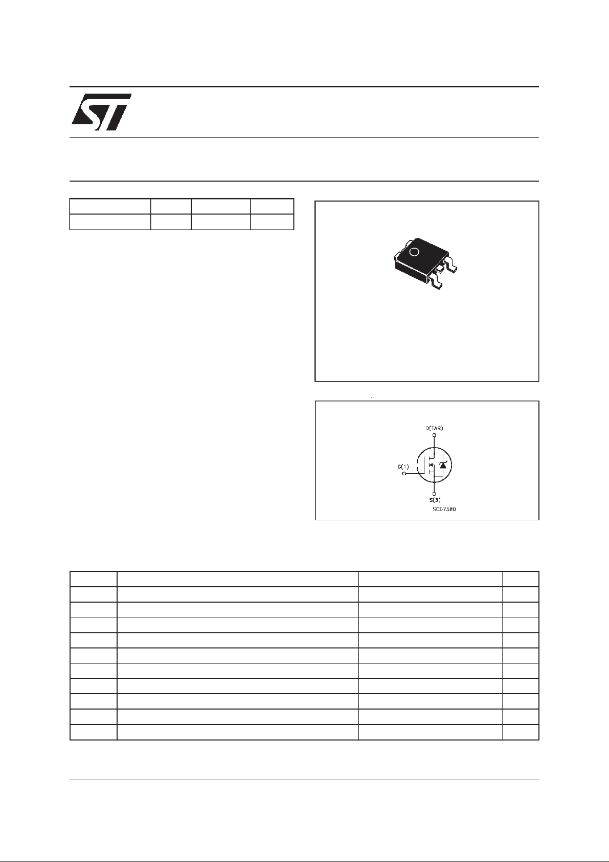
1
DPAK
TO-252
(Suffix ”T4”)
ADD SUFFIX ”T4” FOR ORDERING IN TAPE & REEL
INTERNAL SCHEMATIC DIAGRAM
ABSOLUTE MAXIMUM RATINGS
Symbol Parameter Value Unit
V
V
V
I
DM
P
T
(•) Pulse widthlimited by safe operating area
May 2000
Dra in- sour c e V ol t age (VGS=0) 30 V
DS
Dra in- gate Vol t age (RGS=20kΩ)30V
DGR
Gat e-sourc e Volt age
GS
I
Dra in Curr ent (c ont in uous ) at Tc=25oC40A
D
I
Dra in Curr ent (c ont in uous ) at Tc=100oC28A
D
(•) Dra in Curr ent (puls ed ) 160 A
Tot al Diss ipation at Tc=25oC55W
tot
Der ati ng F ac t or 0.37 W/
St orage T emperature -65 to 175
stg
T
Max. Oper at ing J unction Tem peratur e 175
j
15 V
±
o
C
o
C
o
C
1/6
STD40NF3LL
THERMAL DATA
R
thj-case
R
thj-amb
T
Ther mal Resistanc e Junct ion-case Max
Ther mal Resistanc e Junct ion-ambie nt Max
Maximum L ead Tempe rat ur e For Soldering Purp os e
l
2.73
62.5
300
o
C/W
o
C/W
o
C
ELECTRICAL CHARACTERISTICS
=25oC unless otherwisespecified)
(T
case
OFF
Symbol Parameter Test Conditions Min. Typ. Max. U nit
V
(BR)DSS
Drain-source
ID=250µAVGS=0 30 V
Break dow n Volt age
I
DSS
I
GSS
Zero Gate Voltage
Drain Current (V
GS
Gat e- bod y L eak ag e
Current (V
DS
=0)
=0)
V
=MaxRating
DS
=MaxRating Tc=125oC
V
DS
V
= ± 20 V ± 100 nA
GS
1
10
ON(∗)
Symbol Parameter Test Conditions Min. Typ. Max. U nit
V
GS(th)
R
DS(on)
I
D(on)
Gate Threshold Voltage VDS=VGSID= 250 µ A12.5V
Sta t ic Drain -s ource On
Resistance
On State Drain Current VDS>I
VGS=10V ID=20A
V
=4.5V ID=10A
GS
D(on)xRDS(on)max
0.0095
0.0115
0.0115
0.0135
40 A
VGS=10V
DYNAMIC
Symbol Parameter Test Conditions Min. Typ. Max. U nit
g
(∗)Forward
fs
Tr ansc on duc tance
C
C
C
Input C apaci t anc e
iss
Out put Capacit anc e
oss
Reverse Tr ansfer
rss
Capacit a nc e
VDS>I
D(on)xRDS(on)maxID
=20 A 40 S
VDS=25V f=1MHz VGS= 0 1700
500
115
µA
µ
Ω
Ω
pF
pF
pF
A
2/6
 Loading...