

STD40NF06
N-CHANNEL 60V - 0.024 Ω - 40A DPAK
STripFET™ II POWER MOSFET
TYPE
V
DSS
STD40NF06 60 V <0.028
■ TYPICAL R
■ EXCEPTIONA L dv/d t CAPABILITY
■ 100% AVALANCHE TESTED
■ SURFACE-MOUNTING DPAK (TO-252)
(on) = 0.024 Ω
DS
R
DS(on)
I
D
40 A
Ω
POWER PACKAGE IN TAPE & REEL
(SUFFIX “T4")
DESCRIPTION
This Power MOSFET is the latest development of
STMicroelectron is unique "Single Feature Size™" str ipbased process . The res ulting tran sistor sho ws extrem ely
high packing density for low on-resistance, rugged
avalanche characteristics and less critical alignment
steps therefore a remarkable manufacturing
reproducibility.
APPLICATIONS
■ HIGH CURRENT, HIGH SWITCHING SPEED
■ MOTOR CONTROL , AUDIO AMPLIFIERS
■ SOLENOID AND RELAY DRIVERS
■ DC-DC & DC-AC CONVERTERS
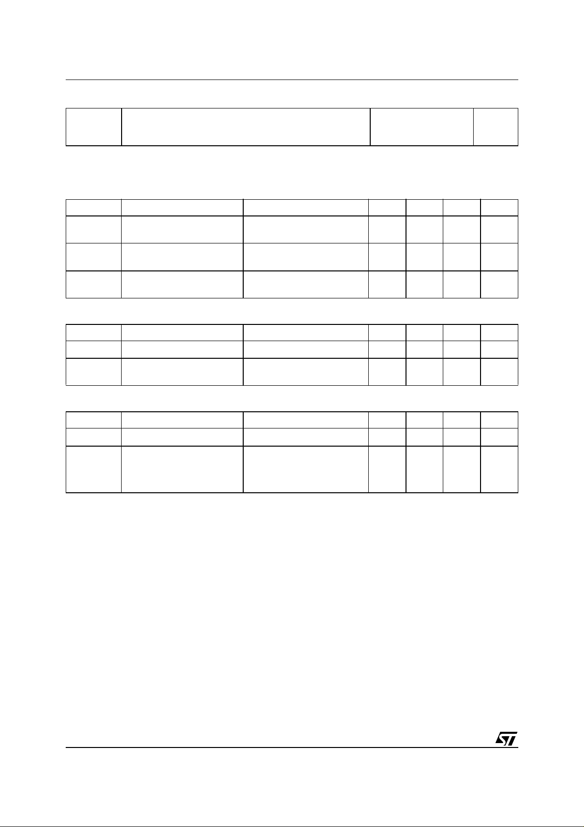
3
1
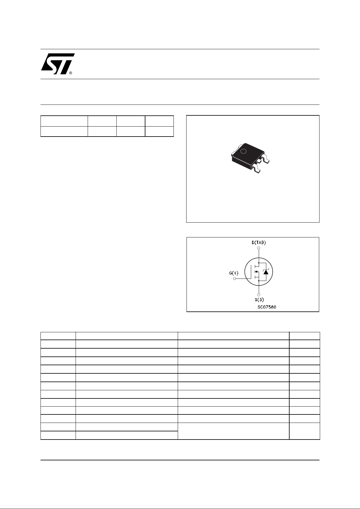
DPAK
TO-252
(Suffix “T4”)
INTERNAL SCHEMATIC DIAGRAM
ABSOLUTE MAXIMUM RATINGS
Symbol Parameter Value Unit
V
DS
V
DGR
V
GS
I
D
I
D
(
I
DM
P
tot
dv/dt
E
AS
T
stg
T
j
(
Pulse width l i mited by safe operating area. (1) ISD ≤40A, di/dt ≤300A/ µ s , VDD ≤ V
•)
Drain-source Voltage (VGS = 0)
Drain-gate Voltage (RGS = 20 kΩ)
60 V
60 V
Gate- source Voltage ± 20 V
Drain Current (continuous) at TC = 25°C
Drain Current (continuous) at TC = 100°C
•)
Drain Current (pulsed) 160 A
Total Dissipation at TC = 25°C
40 A
28 A
85 W
Derating Factor 0.57 W/°C
(1) Peak Diode Recovery voltage slope 10 V/ns
(2)
Single Pulse Avalanche Energy 250 mJ
Storage Temperature
Operating Junction Temperature
(2) Starting Tj = 25 oC, ID = 20 A, VDD = 30 V
-55 to 175 °C
, Tj ≤ T
(BR)DSS
JMAX
1/9January 2003
STD40NF06
THERMA L D ATA
Rthj-case
Rthj-
T
(#) When M ounted on 1 inch
Thermal Resistance Junction-case
Thermal Resistance Junction-PCB (#)
PCB
Maximum Lead Temperature For Soldering Purpose
l
2
FR-4 boar d, 2 oz Cu.
Max
Max
1.76
50
275
°C/W
°C/W
°C
ELECTRICAL CHARACTERISTICS (T
= 25 °C unless otherwise specified)
case
OFF
Symbol Parameter Test Conditions Min. Typ. Max. Unit
I
V
(BR)DSS
Drain-source
= 250 µA, VGS = 0
D
60 V
Breakdown Voltage
V
= Max Rating
DS
V
= Max Rating TC = 100°C
DS
V
= ± 20 V
GS
1
10
±100 nA
ON
(*)
I
DSS
I
GSS
Zero Gate Voltage
Drain Current (V
GS
Gate-body Leakage
Current (V
DS
= 0)
= 0)
Symbol Parameter Test Conditions Min. Typ. Max. Unit
V
V
GS(th)
R
DS(on)
Gate Threshold Voltage
Static Drain-source On
Resistance
= VGS I
DS
V
= 10 V ID = 20 A
GS
= 250 µA
D
24V
0.024 0.028
DYNAMIC
Symbol Parameter Test Conditions Min. Typ. Max. Unit
(*)
g
fs
C
iss
C
oss
C
rss
Forward Transconductance
Input Capacitance
Output Capacitance
Reverse Transfer
Capacitance
V
= 30 V ID= 20 A
DS
= 25V, f = 1 MHz, VGS = 0
V
DS
13 S
920
225
80
µA
µA
Ω
pF
pF
pF
2/9
STD40NF06
ELECTRICAL CHARACTERISTICS (continued)
SWITCHING ON
Symbol Parameter Test Conditions Min. Typ. Max. Unit
= 30 V ID = 20 A
t
d(on)
Turn-on Delay Time
t
r
Rise Time
V
DD
R
= 4.7 Ω VGS = 10 V
G
(Resistive Load, Figure 3)
Q
g
Q
gs
Q
gd
Total Gate Charge
Gate-Source Charge
Gate-Drain Charge
= 48V ID = 40A VGS= 10V
V
DD
SWITCHING OFF
Symbol Parameter Test Conditions Min. Typ. Max. Unit
= 30 V ID = 20 A
t
d(off)
Turn-off Delay Time
t
f
Fall Time
V
DD
R
= 4.7Ω, V
G
GS
= 10 V
(Resistive Load, Figure 3)
SOURCE DRAIN DIODE
Symbol Parameter Test Conditions Min. Typ. Max. Unit
I
SD
I
SDM
V
SD
t
rr
Q
rr
I
RRM
(*)
Pulsed: P ul se duration = 300 µs, duty cy cle 1.5 %.
(
•)Pulse width limited by safe operating area.
Source-drain Current
(•)
Source-drain Current (pulsed)
(*)
Forward On Voltage
Reverse Recovery Time
Reverse Recovery Charge
Reverse Recovery Current
I
= 40 A VGS = 0
SD
= 40 A di/dt = 100A/µs
I
SD
V
= 10 V Tj = 150°C
DD
(see test circuit, Figure 5)
11
50
32
6.5
15
27
11
63
150
4.8
43 nC
40
160
1.3 V
ns
ns
nC
nC
ns
ns
A
A
ns
nC
A
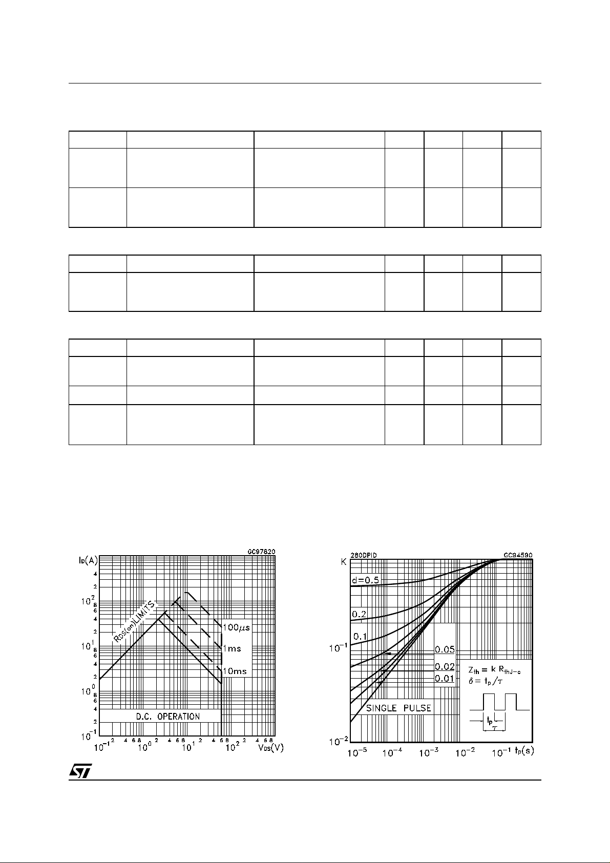
Safe Operating Area Thermal Impedance
3/9

STD40NF06
Output Characteristics Transfer Characteristics
Transconductance Static Drain-source On Resistance
Gate Charge vs Gate-source Voltage Capacitance Variations
4/9

STD40NF06
Normalized Gate Threshold Voltage vs Temperature Normalized on Resistance vs Temperature
Source-drain Diode Forward Characteristics Normalized Breakdown Voltage vs Temperature.
. .
5/9

STD40NF06
Fig. 1: Unclamped Inductive Load Test CircuitFig. 1: Unclamped Inductive Load Test Circuit Fig. 2: Unclamped Inductive Waveform
Fig. 3: Switching Times Test Circuits For Resistive
Load
Fig. 5: Test Circuit For Inductive Load Switching
And Diode Recovery Times
Fig. 4: Gate Charge test Circuit
6/9

TO-252 (DPAK) MECHANICAL DATA
STD40NF06
DIM.
mm inch
MIN. TYP. MAX. MIN. TYP. MAX.
A 2.2 2.4 0.086 0.094
A1 0.9 1.1 0.035 0.043
A2 0.03 0.23 0.001 0.009
B 0.64 0.9 0.025 0.035
B2 5.2 5.4 0.204 0.212
C 0.45 0.6 0.017 0.023
C2 0.48 0.6 0.019 0.023
D 6 6.2 0.236 0.244
E 6.4 6.6 0.252 0.260
G 4.4 4.6 0.173 0.181
H 9.35 10.1 0.368 0.397
L2 0.8 0.031
L4 0.6 1 0.023 0.039
A
C2
L2
E
B2
==
H
DETAIL "A"
D
==
C
B
2
1 3
L4
A1
G
==
A2
DETAIL "A"
0068772-B
7/9

STD40NF06
*on sales ty pe
8/9

STD40NF06
Information furnished is believed to be accurate and reliable. However, STMicroelectronics assumes no responsibility for the consequences
of use of such information nor for any infringement of patents or other rights of third parties which may result from its use. No license is granted
by implic ation or oth erwise under any pat ent or patent rights of STMicroe l ectronics. S pecificat i ons mentioned in this publicati on are subject
to change without notice. This publication supersedes and replaces all information previously supplied. STMicroelectronics product s are not
authorized for use as cri t i cal compone nt s i n l i f e support dev i ces or systems wi thout express written approval of STM i croelectr onics.
The ST logo is registered trademark of STMicroelectronics
2002 STMi croelectr oni cs - All Righ ts Reserved
All other na m es are the prop erty of their respective owners.
Australi a - Brazil - Canada - China - F i nl and - Franc e - Germany - Hong Kong - Ind ia - Is rael - Italy - Japan - Malay sia - Malta - Morocco -
Singap ore - Spain - Sweden - Switzerland - Uni ted Kingdom - United States.
STMicroelectronics GROUP OF COMPANIES
http:// www.st.com
9/9
 Loading...