

SGS Thomson Microelectronics STP4NM60, STD3NM60-1, STD3NM60 Datasheet
STP4NM60
3
STD3NM60 - STD3NM60-1
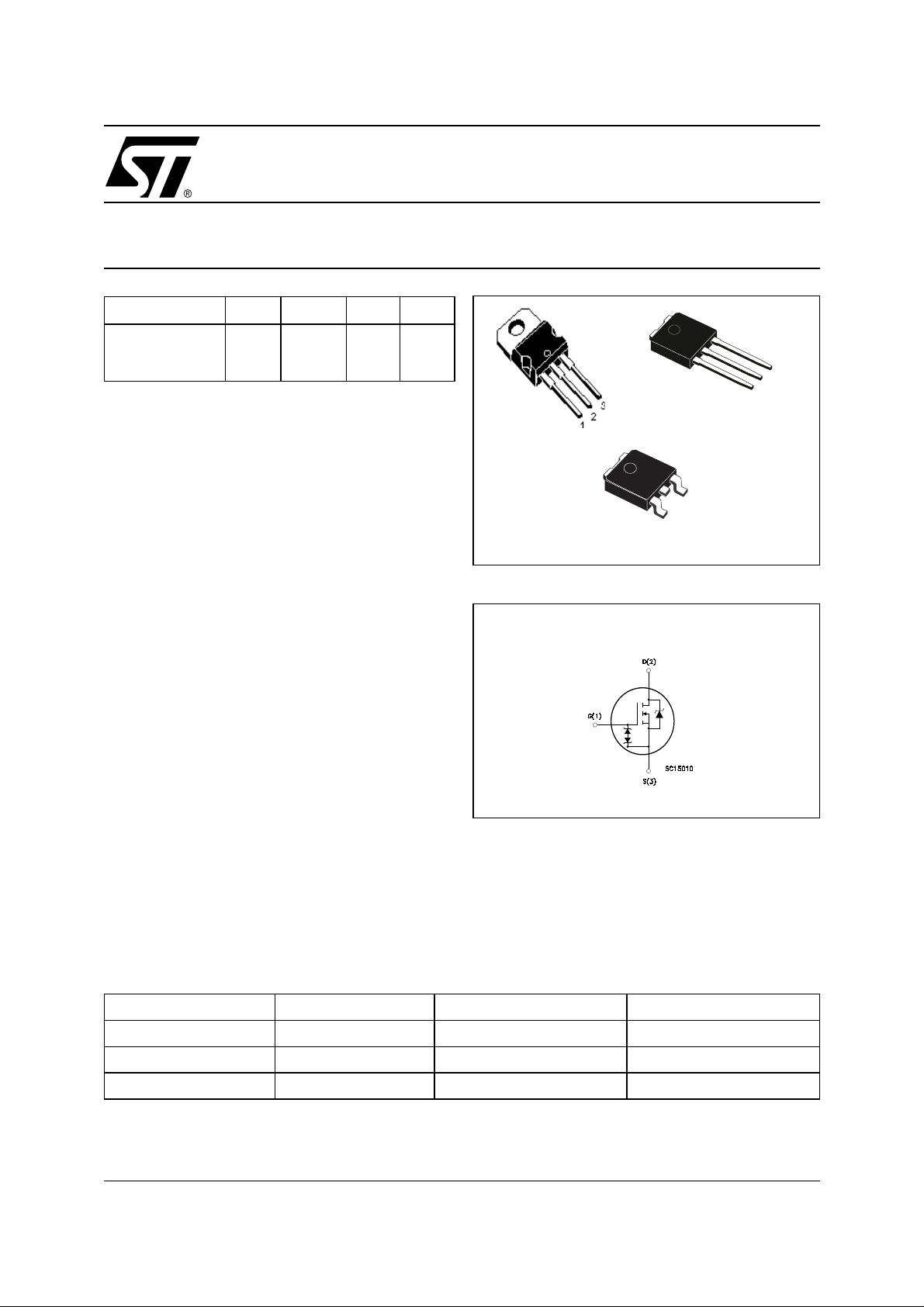
N-CHANNEL 600V - 1.3Ω - 3A TO-220/DPAK/IPAK
Zener-Protected MDmesh™Power MOSFET
TYPE V
STP4NM60
STD3NM60
STD3NM60-1
■ TYPICAL R
■ HIGH dv/dt AND AVALANCHE CAPABILITIES
■ IMPROVED ESD CAPABILITY
■ LOW INPUT CAPACITANCE AND GATE
600 V
600 V
600 V
(on) = 1.3 Ω
DS
DSS
R
DS(on)
< 1.5 Ω
< 1.5 Ω
< 1.5 Ω
I
D
4 A
3 A
3 A
Pw
69 W
42 W
42 W
CHARGE
■ LOW GATE INPUT RESIST ANC E
■ TIGHT PROCESS CONTROL AND HIGH
MANUFACTORING YIELDS
DESCRIPTION
The MDmesh™
is a new revolutionary MOSFET
technology that associates the Multiple Drain process with the Company’s PowerMESH™ horizontal
layout. The resulting product has an outstanding low
on-resistance, impressively high dv/dt and excellent
avalanche characteristics. The adoption of the
Company’s proprietary strip technique yields overall
dynamic performance that is significantly better than
that of similar completition’s products.
IPAK
TO-220
3
1
DPAK
INTERNAL SCHEMATIC DIAGRAM
2
1
APPLICATIONS
The MDmesh™ family is very suitable for increase
the power density of high voltage converters allowing system miniaturization and higher efficiencies.
ORDERING INFORMATION
SALES TYPE MARKING PACKAGE PACKAGING
STP4NM60 P4NM60 TO-220 TUBE
STD3NM60T4 D3NM60 DPAK TAPE & REEL
STD3NM60-1 D3NM60 IPAK TUBE
1/12September 2002

STP4NM60 / STD3NM60 / STD3NM60-1
ABSOLUTE MAXIMUM RATINGS
Symbol Parameter Value Unit
STP4NM60
V
DS
V
DGR
V
GS
I
D
I
D
I
DM
P
TOT
Drain-source Voltage (VGS = 0)
Drain-gate Voltage (RGS = 20 kΩ)
600 V
600 V
Gate- source Voltage ± 30 V
Drain Current (continuous) at TC = 25°C
Drain Current (continuous) at TC = 100°C
(l)
Drain Current (pulsed) 16 12 A
Total Dissipation at TC = 25°C
43A
2.52 1.9 A
69 42 W
Derating Factor 0.55 0.33 W/°C
dv/dt (1) Peak Diode Recovery voltage slope 15 V/ns
T
j
T
stg
(l) Pulse wi dth limited by safe operating area
(1) I
≤3A, di/dt ≤400 µA, VDD ≤ V
SD
Operating Junction Temperature
Storage Temperature
, Tj ≤ T
(BR)DSS
JMAX.
-65 to 150
-65 to 150
THERMA L D ATA
TO-220
Rthj-case Thermal Resistance Junction-case Max 1.82 3 °C/W
Rthj-amb Thermal Resistance Junction-ambient Max 62.5 °C/W
T
l
Maximum Lead Temperature For Soldering Purpose
300 °C
STD3NM60
STD3NM60-1
DPAK
IPAK
°C
°C
AVALANCHE CHARACTERISTICS
Symbol Parameter Max Value Unit
I
AR
E
AS
Avalanche Current, Repetitive or Not-Repetitive
(pulse width limited by T
max)
j
Single Pulse Avalanche Energy
(starting T
= 25 °C, ID = IAR, VDD = 50 V)
j
1.5 A
200 mJ
GATE-SOURCE ZENER DIODE
Symbol Parameter Test Conditions Min. Typ. Max. Unit
BV
GSO
Gate-Source Breakdown
Igs=± 1mA (Open Drain) 30 V
Voltage
PROTECTION FEATURES OF GATE-TO-SOURCE ZENER DIODES
The built-in back-to-back Zener diodes have specifically been designed to enhance not only the device’s
ESD capability, but also to make them safely absorb possible voltage transients that may occasionally be
applied from gate to source. In this respect the Zener voltage is appropriate to achieve an efficient and
cost-effective intervention to protect the device’s integrity. These integrated Zener diodes thus avoid the
usage of external components.
2/12
STP4NM60 / STD3NM 60 / STD3NM60-1
ELECTRICAL CHARACTERISTICS (T
=25°C UNLESS OTHERWISE SPECIFIED)
CASE
ON/OFF
Symbol Parameter Test Conditions Min. Typ. Max. Unit
V
(BR)DSS
Drain-source
ID = 250 µA, VGS = 0 600 V
Breakdown Voltage
I
DSS
I
GSS
V
GS(th)
R
DS(on)
Zero Gate Voltage
Drain Current (V
GS
= 0)
Gate-body Leakage
Current (V
DS
= 0)
Gate Threshold Voltage
Static Drain-source On
V
= Max Rating
DS
VDS = Max Rating, TC = 125 °C
V
= ± 20V ±5 µA
GS
V
= VGS, ID = 250µA
DS
345V
1
10
VGS = 10V, ID = 1.5 A 1.3 1.5 Ω
Resistance
DYNAMIC
Symbol Parameter Test Conditions Min. Typ. Max. Unit
g
(1) Forward Transconductance VDS = 15 V, ID= 1.5 A 2.7 S
fs
C
iss
C
oss
C
rss
Input Capacitance
Output Capacitance
Reverse Transfer
Capacitance
= 25V, f = 1 MHz, VGS = 0 324
V
DS
132
7.4
SWITCHING ON
Symbol Parameter Test Conditions Min. Typ. Max. Unit
t
d(on)
Q
Q
Q
Turn-on Delay Time
t
r
g
gs
gd
Rise Time
Total Gate Charge
Gate-Source Charge
Gate-Drain Charge
VDD = 300 V, ID = 1.5 A
RG= 4.7Ω VGS = 10 V
(Resistive Load see, Figure 3)
= 480V, ID = 3 A,
V
DD
V
= 10V
GS
9
4
10
3
4.7
14
µA
µA
pF
pF
pF
ns
ns
nC
nC
nC
SWITCHING OFF
Symbol Parameter Test Conditions Min. Typ. Max. Unit
= 480 V, ID = 3 A,
t
r(Voff)
t
t
Off-voltage Rise Time
f
c
Fall Time
Cross-over Time
V
DD
RG=4.7Ω, V
GS
= 10V
(Inductive Load see, Figure 5)
16.5
10.5
15
SOURCE DRAIN DIODE
Symbol Parameter Test Conditions Min. Typ. Max. Unit
I
SD
I
SDM
VSD (1)
t
rr
Q
rr
I
RRM
t
rr
Q
rr
I
RRM
Note: 1. Pulsed: Pu l se duration = 300 µs, duty c ycle 1.5 %.
2. Pulse width li mited by safe operating area.
Source-drain Current
(2)
Source-drain Current (pulsed)
Forward On Voltage
Reverse Recovery Time
Reverse Recovery Charge
Reverse Recovery Current
Reverse Recovery Time
Reverse Recovery Charge
Reverse Recovery Current
ISD = 3 A, VGS = 0
I
SD
V
DD
(see test circuit, Figure 5)
I
SD
VDD = 100 V, Tj = 150°C
(see test circuit, Figure 5)
= 3 A, di/dt = 100A/µs
= 100 V, Tj = 25°C
= 3 A, di/dt = 100A/µs
224
1
9
296
1.4
9.3
3
12
1.5 V
ns
ns
ns
A
A
ns
µC
A
ns
µC
A
3/12
STP4NM60 / STD3NM60 / STD3NM60-1
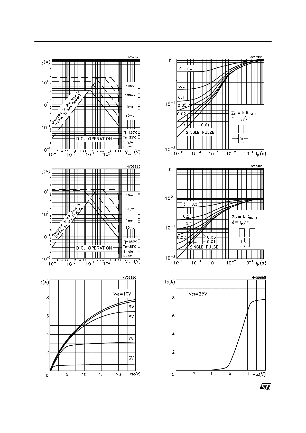
Safe Operating Area For TO-220
Thermal Impedance For TO-220
Thermal Impedance For DPAK / IPAKSafe Operating Area For DPAK / IPAK
Output Characteristics
4/12
Transfer Characteristics
 Loading...