

SGS Thomson Microelectronics STD3NC60 Datasheet
N - CHANNEL 600V - 2 Ω - 3.2A TO-251/TO-252
TYPE V
ST D3 NC6 0 600 V < 2.2 Ω 3.2 A
ν TYPICALR
ν EXTREMELYHIGHdv/dtCAPABILITY
ν 100% AVALANCHETESTED
ν NEWHIGH VOLTAGE BENCHMARK
ν GATECHARGE MINIMIZED
DS(on)
DSS
=2Ω
DESCRIPTION
The PowerMESH is the evolution of the first
generation of MESH OVERLAY. The layout
refinements introduced greatly improve the
Ron*area figure of merit while keepingthe device
at the leading edge for what concerns switching
speed, gate chargeand ruggedness.
APPLICATIONS
ν HIGH CURRENT, HIGH SPEEDSWITCHING
ν SWITHMODE POWERSUPPLIES (SMPS)
ν DC-AC CONVERTERSFORWELDING
EQUIPMENTANDUNINTERRUPTIBLE
POWERSUPPLIESAND MOTORDRIVER
R
DS(on)
I
D
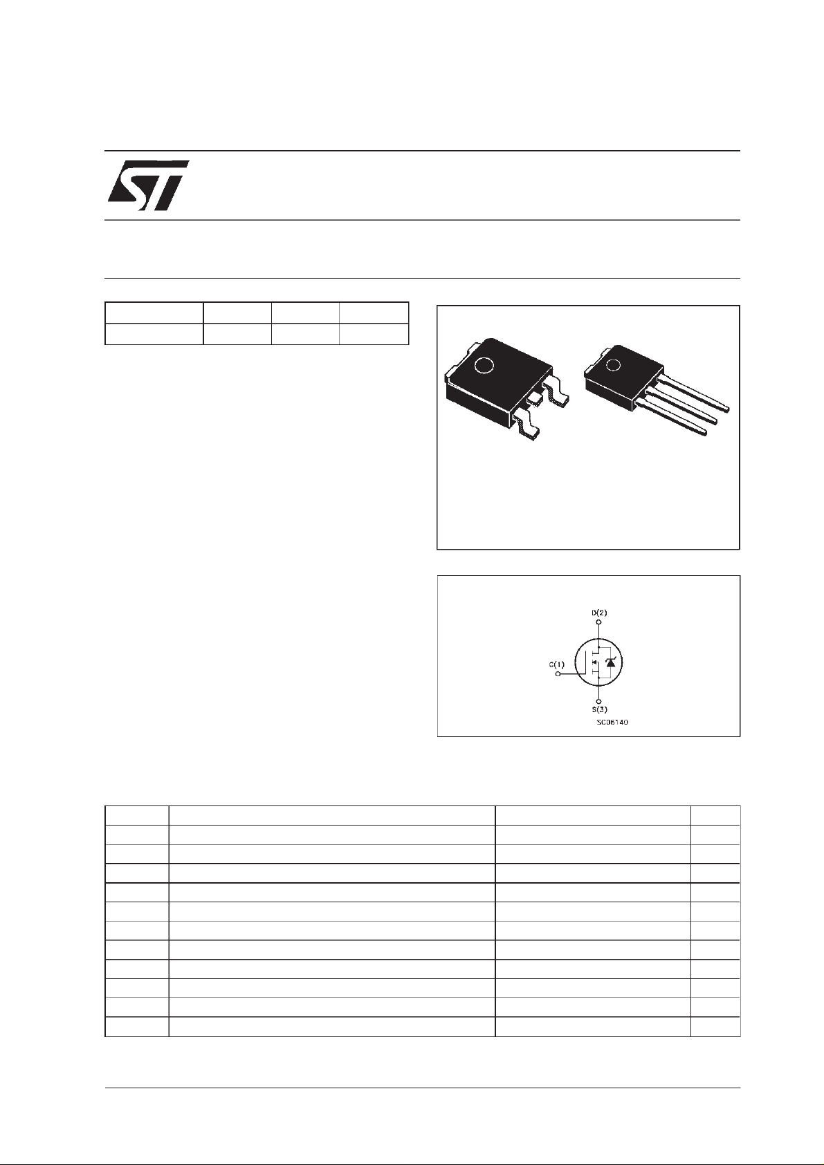
STD3NC60
PowerMESH MOSFET
PRELIMINARY DATA
3
1
DPAK
TO-252
(Suffix ”T4”)
INTERNAL SCHEMATIC DIAGRAM
IPAK
TO-251
(Suffix”-1”)
2
1
3
ABSOLUTE MAXIMUM RATINGS
Symbol Parameter Value Uni t
V
V
V
I
DM
P
dv/dt(
T
February 2000
Drain-source Vol t age (VGS= 0) 600 V
DS
Drain- gat e Voltage (RGS=20kΩ)
DGR
Gate-s ource Voltage ± 30 V
GS
Drain Curr ent (cont in uous ) at Tc=25oC 3.2 A
I
D
Drain Curr ent (cont in uous ) at Tc= 100oC2A
I
D
(•) Drain Current (pulsed) 12.8 A
Tot al Diss ipat i on at Tc=25oC50W
tot
Derating Factor 0.4 W/
1) Peak Diode Rec overy voltage slope 3 V/ns
St orage Te mper ature -65 to 150
stg
Max. Operating Ju nction T emperature 150
T
j
600 V
o
C
o
C
o
C
1/8
STD3NC60
THERMAL DATA
R
thj-cas e
Rthj-amb
R
thc-sin k
T
AVALANCHE CHARACTERISTICS
Symb ol Parameter Max Val ue Uni t
I
AR
E
Therma l Resistan ce Juncti on-c as e Max
Therma l Resistan ce Juncti on-am b ien t Max
Therma l Resistan ce Case-sink Typ
Maxim um Lead Temperature For Sol dering P urpose
l
Avalanc h e Cur rent , Repetit ive or N ot-Repet it ive
(pulse width li mit ed by T
Single Puls e A valanche Energy
AS
(starting T
=25oC, ID=IAR,VDD=50V)
j
max)
j
2.5
100
1.5
275
3.2 A
220 mJ
o
C/W
oC/W
o
C/W
o
C
ELECTRICAL CHARACTERISTICS (T
=25oC unlessotherwisespecified)
case
OFF
Symb ol Parameter Test Conditions Mi n . Typ . Max. Unit
V
(BR) DSS
Drain-s ource
= 250 µ AVGS=0
I
D
600 V
Break down Voltage
I
DSS
I
GSS
Zero Gate Voltage
Drain Curre nt (V
GS
Gate-body Leak a ge
Current (V
DS
=0)
=0)
V
=MaxRating
DS
= Max Rating Tc= 125oC
V
DS
= ± 30 V
V
GS
1
50
± 100 nA
ON (∗)
Symb ol Parameter Test Conditions Mi n . Typ . Max. Unit
V
GS(th)
R
DS(on)
Gate Threshold Voltage
Static Drain- s ource O n
V
DS=VGSID
=250µA
VGS= 10V ID=1.5A 2 2.2 Ω
234V
Resistance
I
D(on)
On State Drain Current VDS>I
D(on)xRDS(on)max
3.2 A
VGS=10V
DYNAMIC
Symb ol Parameter Test Conditions Mi n . Typ . Max. Unit
g
(∗)Forward
fs
Transconductanc e
Input Capacit anc e
iss
Output Capacitance
Reverse Transfer
rss
C
C
oss
C
Capacit ance
VDS>I
D(on)xRDS(on)maxID
=1.5A 2 S
VDS=25V f=1MHz VGS= 0 700
85
9
µA
µA
pF
pF
pF
2/8
STD3NC60
ELECTRICAL CHARACTERISTICS (continued)
SWITCHING ON
Symb ol Parameter Test Conditions Mi n . Typ . Max. Unit
t
d(on)
t
r
Turn-on T ime
Rise Time
VDD=300V ID=1.5A
=4.7 Ω VGS=10V
R
G
(see test circuit, figure 3)
Q
Q
Q
Total Gate Charge
g
Gate-Source Charge
gs
Gate-Drain Charge
gd
VDD=480V ID=3.2A VGS=10V 18
SWITCHING OFF
Symb ol Parameter Test Conditions Mi n . Typ . Max. Unit
t
r(Voff)
t
t
Off -voltag e Rise Time
Fall T ime
f
Cross -over Time
c
VDD=480V ID=3.2A
=4.7 Ω VGS=10V
R
G
(see test circuit, figure 5)
SOURCEDRAINDIODE
Symb ol Parameter Test Conditions Mi n . Typ . Max. Unit
I
SD
I
SDM
V
SD
t
Q
I
RRM
(∗) Pulsed: Pulse duration = 300µs, dutycycle 1.5 %
(•) Pulse width limitedby safe operatingarea
Source-drain Current
(•)
Source-drain Current
(pulsed)
(∗)ForwardOnVoltage ISD=3.2A VGS=0 1.6 V
Revers e Recover y
rr
Time
Revers e Recover y
rr
=3.2A di/dt=100A/µs
I
SD
=100V Tj= 150oC
V
DD
(see test circuit, figure 5)
Charge
Revers e Recover y
Current
14
11
25 nC
6
8
10
8
7
3.2
12.8
610
3.6
11.7
ns
ns
nC
nC
ns
ns
ns
A
A
ns
µC
A
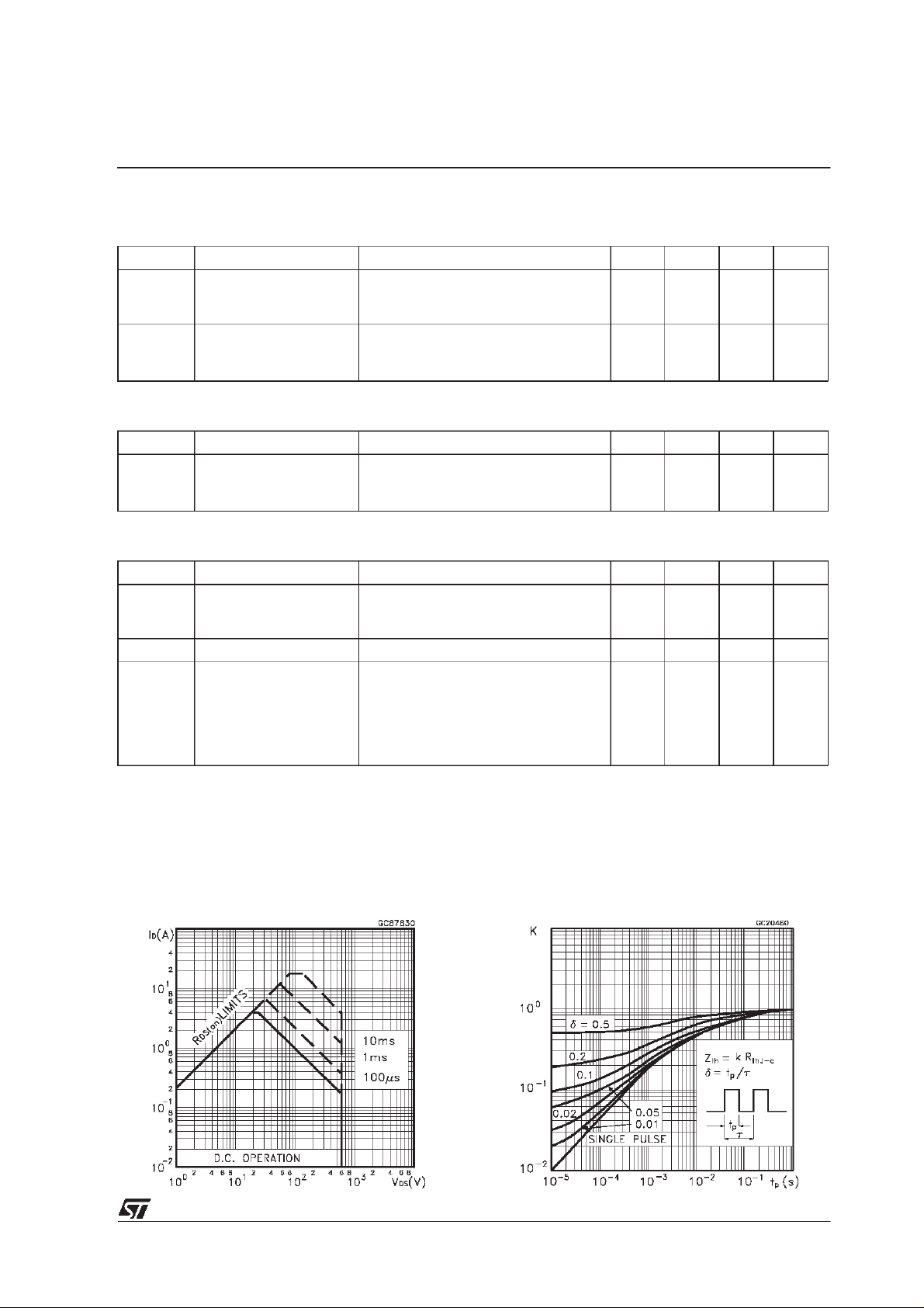
Safe Operating Area Thermal Impedance
3/8
 Loading...