

SGS Thomson Microelectronics STD3NC50 Datasheet
N - CHANNEL 500V - 2.4Ω - 3A TO-251/TO-252
TYPE V
DSS
ST D3N C50 50 0 V < 2.7 Ω 3A
■ TYPICALR
■ EXTREMELYHIGH dv/dt CAPABILITY
■ 100%AVALANCHETESTED
■ NEWHIGH VOLTAGE BENCHMARK
■ GATECHARGE MINIMIZED
■ ADDSUFFIX ”T4” FORORDERING INTAPE
DS(on)
= 2.4 Ω
& REEL.
R
DS(on)
I
D
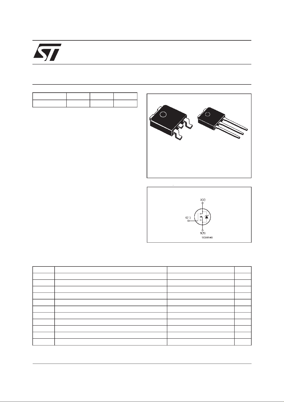
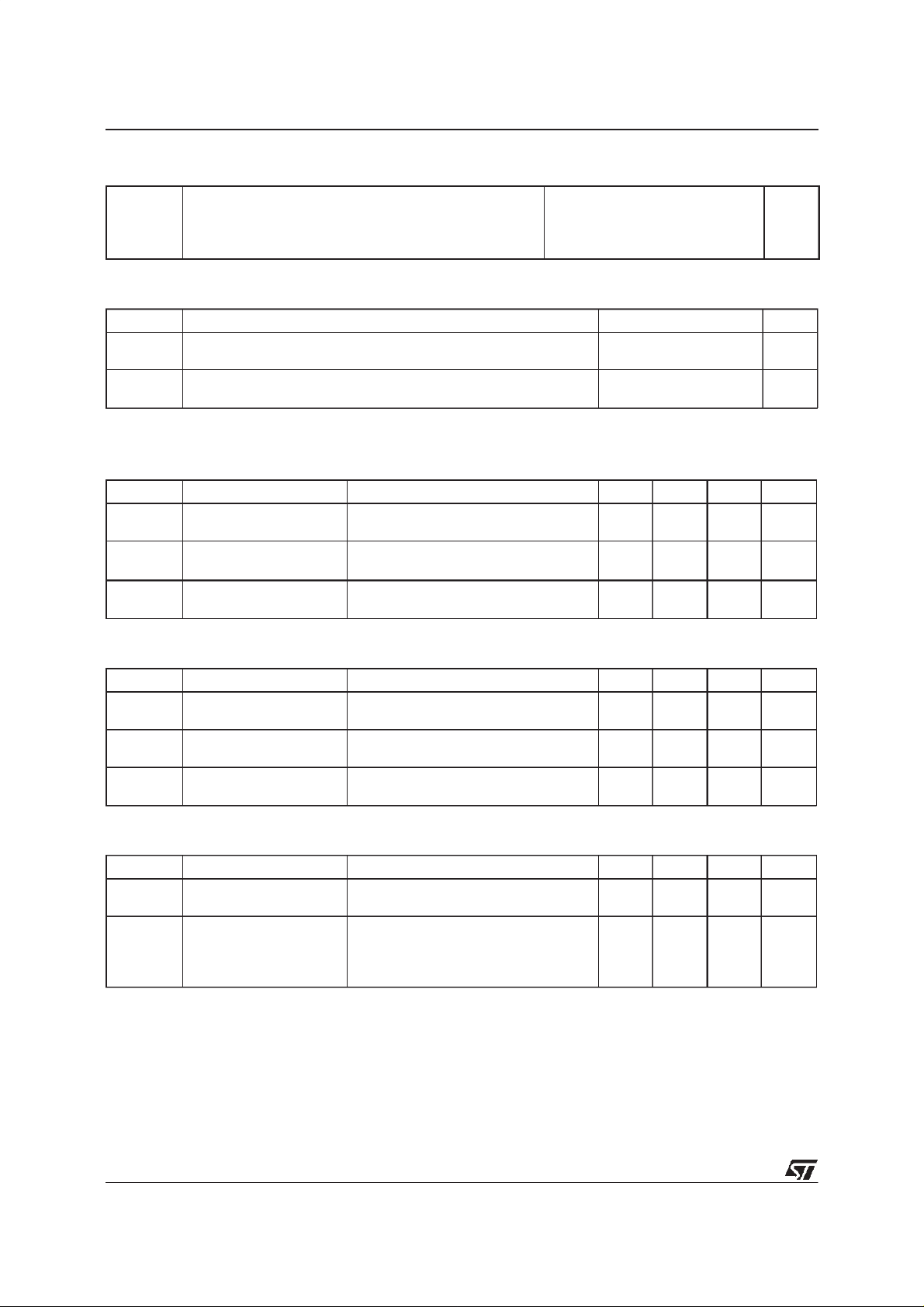
STD3NC50
PowerMESH ΙΙ MOSFET
PRELIMINARY DATA
3
1
2
1
3
DESCRIPTION
The PowerMESH
is the evolution of the first
ΙΙ
generation of MESH OVERLAY. The layout
DPAK
TO-252
(Suffix ”T4”)
IPAK
TO-251
(Suffix”-1”)
refinements introduced greatly improve the
Ron*areafigure of meritwhile keeping the device
at the leading edge for what concerns switching
speed,gate chargeand ruggedness.
INTERNAL SCHEMATIC DIAGRAM
APPLICATIONS
■ HIGHCURRENT, HIGH SPEEDSWITCHING
■ SWITHMODE POWER SUPPLIES (SMPS)
■ DC-AC CONVERTERS FOR WELDING
EQUIPMENTAND UNINTERRUPTIBLE
POWERSUPPLIESAND MOTORDRIVER
ABSOLUTE MAXIMUM RATINGS
Symbol Parameter Value Unit
V
V
V
I
DM
P
dv/ dt(
T
(•) Pulse width limited by safe operating area (1)ISD≤3 A, di/dt ≤ 100 A/µs, VDD≤ V
Drain-source Voltage (VGS=0) 500 V
DS
Dra in- gate Voltage (RGS=20kΩ)
DGR
Gate -sourc e Voltage
GS
Drain Current (continuous) at Tc=25oC3.2A
I
D
Drain Current (continuous) at Tc=100oC2A
I
D
500 V
30 V
±
(•) Drain Current (pulsed) 12.8 A
Total Dissipation at Tc=25oC60W
tot
Derating Factor 0.48 W/
1) P eak Dio de Recovery volt age slope 4 V/ns
St orage Tempe rature -65 to 150
stg
Max. Op erating Junc t ion T e m pe rat ure 150
T
j
,Tj≤T
(BR)DSS
JMAX
o
C
o
C
o
C
January 2000
1/7
STD3NC50
THERMAL DATA
R
thj-case
Rthj-amb
R
thc-sink
T
AVALANCHE CHARACTERISTICS
Symbol Para meter Max Val ue Uni t
I
AR
E
Ther mal Resist an c e J unction- case Max
Ther mal Resist an c e J unction- ambient Max
Thermal Resistance Case-sink Typ
Maximum Lead Tem perature Fo r Soldering P urpose
l
Avalanche Curr ent, Repetit ive or Not-Re petitive
(pulse width limited by T
Single Pu lse Avalanche Energy
AS
(starting T
=25oC, ID=IAR,VDD=50V)
j
max)
j
2.0
100
1.5
275
3A
40 mJ
o
C/W
oC/W
o
C/W
o
C
ELECTRICAL CHARACTERISTICS (T
=25oC unless otherwisespecified)
case
OFF
Symbol Parameter Test Conditions Min. Typ. Max. Unit
V
(BR)DSS
Drain-source
=250µAVGS=0
I
D
500 V
Break d own V o lt age
I
DSS
I
GSS
Zero Gate Voltage
Drain Cu rr ent (V
GS
Gat e- b ody Le akage
Current (V
DS
=0)
=0)
V
=MaxRating
DS
= Max Rating Tc=125oC
V
DS
= ± 30 V
V
GS
1
50
± 100 nA
ON(∗)
Symbol Parameter Test Conditions Min. Typ. Max. Unit
V
GS(th)
Gate Threshold
V
DS=VGSID
= 250 µA
234V
Voltage
R
DS(on)
Static Drain-source On
VGS=10V ID= 1.5 A 2.4 2.7
Resistance
I
D(on)
On Stat e D ra in Curr ent VDS>I
D(on)xRDS(on)max
3A
VGS=10V
DYNAMIC
Symbol Parameter Test Conditions Min. Typ. Max. Unit
g
(∗)Forward
fs
Tr ansconductance
C
C
C
Input Cap ac i t an c e
iss
Out put Capacitanc e
oss
Reverse Transf er
rss
Capacitance
VDS>I
D(on)xRDS(on)maxID
=1.5A 2 S
VDS=25V f=1MHz VGS=0 400
62
7.5
µA
µ
Ω
pF
pF
pF
A
2/7
STD3NC50
ELECTRICAL CHARACTERISTICS
(continued)
SWITCHINGON
Symbol Parameter Test Conditions Min. Typ. Max. Unit
t
d(on)
Q
Q
Q
Turn-on Time
t
Rise Time
r
Total Gate Charge
g
Gat e- Source Char ge
gs
Gate-Drain Charge
gd
VDD= 300 V ID=1.5A
R
=4.7
G
Ω
VGS=10V
VDD= 480 V ID=3A VGS=10V 15
11
8
21 nC
6.5
5
SWITCHINGOFF
Symbol Parameter Test Conditions Min. Typ. Max. Unit
t
r(Voff)
t
t
Off -voltage Rise Time
Fall Time
f
Cross-over T i m e
c
VDD= 400 V ID=3A
=4.7 ΩVGS=10V
R
G
8
5
14
SOURCEDRAINDIODE
Symbol Parameter Test Conditions Min. Typ. Max. Unit
I
SD
I
SDM
V
SD
t
Q
I
RRM
(∗) Pulsed: Pulse duration = 300 µs, duty cycle 1.5 %
(•) Pulse width limited by safe operating area
Source-drain Curr ent
(•)
Source-drain Curr ent
3
12
(pulsed)
(∗) For ward On Voltage ISD=3A VGS=0 1.6 V
Reverse Recov ery
rr
Time
Reverse Recov ery
rr
= 3 A d i/ d t = 100 A/µs
I
SD
= 100 V Tj=150oC
V
DD
245
980
Charge
Reverse Recov ery
8
Current
ns
ns
nC
nC
ns
ns
ns
A
A
ns
µ
A
C
3/7
 Loading...