

SGS Thomson Microelectronics STD35NF3LL, STD35NF3LL-1 Datasheet
STD35NF3LL
STD35NF3LL-1
N-CHANNEL 30V - 0.014 Ω - 35A IPAK/DPAK
STripFET™ II POWER MOSFET
TYPE
STD35NF3LL
STD35NF3LL-1
■ TYPICAL R
■ OPTIMAL R
■ CONDUCTION LOSSES REDUCED
■ SWITCHING LOSSES REDUCED
■ LOW THRESHOLD DRIVE
■ THROUGH-HOLE IPAK (TO-251) POWER
DS
DS
V
DSS
30 V
30 V
(on) = 0.016 Ω @ 4.5V
(on) x Qg TRADE-OFF @ 4.5V
R
DS(on)
< 0.0195
< 0.0195
I
D
35 A
Ω
35 A
Ω
PACKAGE IN TUBE (SUFFIX “- 1 ")
■ SURFACE-MOUNTING DPAK (TO-252)
POWER PACKAGE IN TAPE & REEL
(SUFFIX “T4")
DESCRIPTION
This application specific Power MOSFET is the third
genaration of STMicro electronis unique "Single Feature
Size™" strip-based process. The resulting transistor
shows the best trade-off between on-resistance and gate
charge. When used as high and low side in buck
regulators, it gives the be st perfor manc e in terms of both
conduction and switching losses. This is extremely
important for motherboards where fast switching and
high efficiency are of paramount importance.
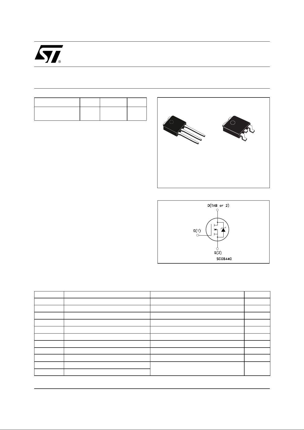
3
2
1
IP AK
TO-251
(Suffix “-1”)
DPAK
TO-252
(Suffix “T4”)
INTERNAL SCHEMATIC DIAGRAM
3
1
APPLICATIONS
■ SPECIFICALL Y D ESIGNED AND OP TIMISED
FOR HIGH EFFICIENCY DC/DC
CONVERTERS
ABSOLUTE MAXIMUM RATINGS
Symbol Parameter Value Unit
V
DS
V
DGR
V
GS
I
D
I
D
(
I
DM
P
tot
E
AS
T
stg
T
j
(
Pulse width limited by safe operating area. (1) Starting Tj = 25 oC, ID = 17.5 A, VDD= 24 V
•)
.
Drain-source Voltage (VGS = 0)
Drain-gate Voltage (RGS = 20 kΩ)
30 V
30 V
Gate- source Voltage ± 16 V
Drain Current (continuos) at TC = 25°C
Drain Current (continuos) at TC = 100°C
•)
Drain Current (pulsed) 140 A
Total Dissipation at TC = 25°C
35 A
25 A
50 W
Derating Factor 0.33 W/°C
(1)
Single Pulse Avalanche Energy 300 mJ
Storage Temperature
Max. Operating Junction Temperature
-55 to 175 °C
1/10February 2002

STD35NF3LL/STD35NF3LL-1
THERMA L D ATA
Rthj-case
Rthj-amb
T
Thermal Resistance Junction-case
Thermal Resistance Junction-ambient
Maximum Lead Temperature For Soldering Purpose
l
Max
Max
Typ
3
100
300
°C/W
°C/W
°C
ELECTRICAL CHARACTERISTICS (T
= 25 °C unless otherwise specified)
case
OFF
Symbol Parameter Test Conditions Min. Typ. Max. Unit
I
V
(BR)DSS
Drain-source
= 250 µA, VGS = 0
D
30 V
Breakdown Voltage
V
= Max Rating
DS
V
= Max Rating TC = 100°C
DS
V
= ± 16 V
GS
1
10
±100 nA
ON
(*)
I
DSS
I
GSS
Zero Gate Voltage
Drain Current (V
GS
Gate-body Leakage
Current (V
DS
= 0)
= 0)
Symbol Parameter Test Conditions Min. Typ. Max. Unit
V
V
GS(th)
R
DS(on)
Gate Threshold Voltage
Static Drain-source On
Resistance
= VGS I
DS
= 10 V ID = 17.5 A
V
GS
V
= 4.5 V ID = 17.5 A
GS
= 250 µA
D
1V
0.014
0.016
0.0195
0.0215
DYNAMIC
Symbol Parameter Test Conditions Min. Typ. Max. Unit
(*)
g
fs
C
iss
C
oss
C
rss
Forward Transconductance
Input Capacitance
Output Capacitance
Reverse Transfer
Capacitance
V
=15 V ID= 17.5 A
DS
= 25V, f = 1 MHz, VGS = 0
V
DS
19 S
800
250
60
µA
µA
Ω
Ω
pF
pF
pF
2/10
STD35NF3LL/STD35NF3LL-1
ELECTRICAL CHARACTERISTICS (continued)
SWITCHING ON
Symbol Parameter Test Conditions Min. Typ. Max. Unit
= 15 V ID = 17.5 A
t
d(on)
Turn-on Delay Time
t
r
Rise Time
V
DD
R
= 4.7 Ω VGS = 4.5 V
G
(Resistive Load, Figure 3)
Q
g
Q
gs
Q
gd
Total Gate Charge
Gate-Source Charge
Gate-Drain Charge
= 24 V ID = 35 A VGS= 5V
V
DD
SWITCHING OFF
Symbol Parameter Test Conditions Min. Typ. Max. Unit
= 15 V ID = 17.5 A
t
d(off)
Turn-off Delay Time
t
f
Fall Time
V
DD
R
= 4.7 Ω V
G
GS
= 4.5 V
(Resistive Load, Figure 3)
SOURCE DRAIN DIODE
Symbol Parameter Test Conditions Min. Typ. Max. Unit
I
SD
I
SDM
V
SD
t
rr
Q
rr
I
RRM
(*)
Pulsed: P ul se duration = 300 µs, duty cycle 1.5 %.
(
•)Pulse width limited by s afe operating area.
Source-drain Current
(•)
Source-drain Current (pulsed)
(*)
Forward On Voltage
Reverse Recovery Time
Reverse Recovery Charge
Reverse Recovery Current
I
= 35 A VGS = 0
SD
= 35 A di/dt = 100A/µs
I
SD
V
= 15 V Tj = 150°C
DD
(see test circuit, Figure 5)
17
100
12.5
4.2
5.2
20
21
35
44
2.5
17 nC
35
140
1.3 V
ns
ns
nC
nC
ns
ns
A
A
ns
nC
A
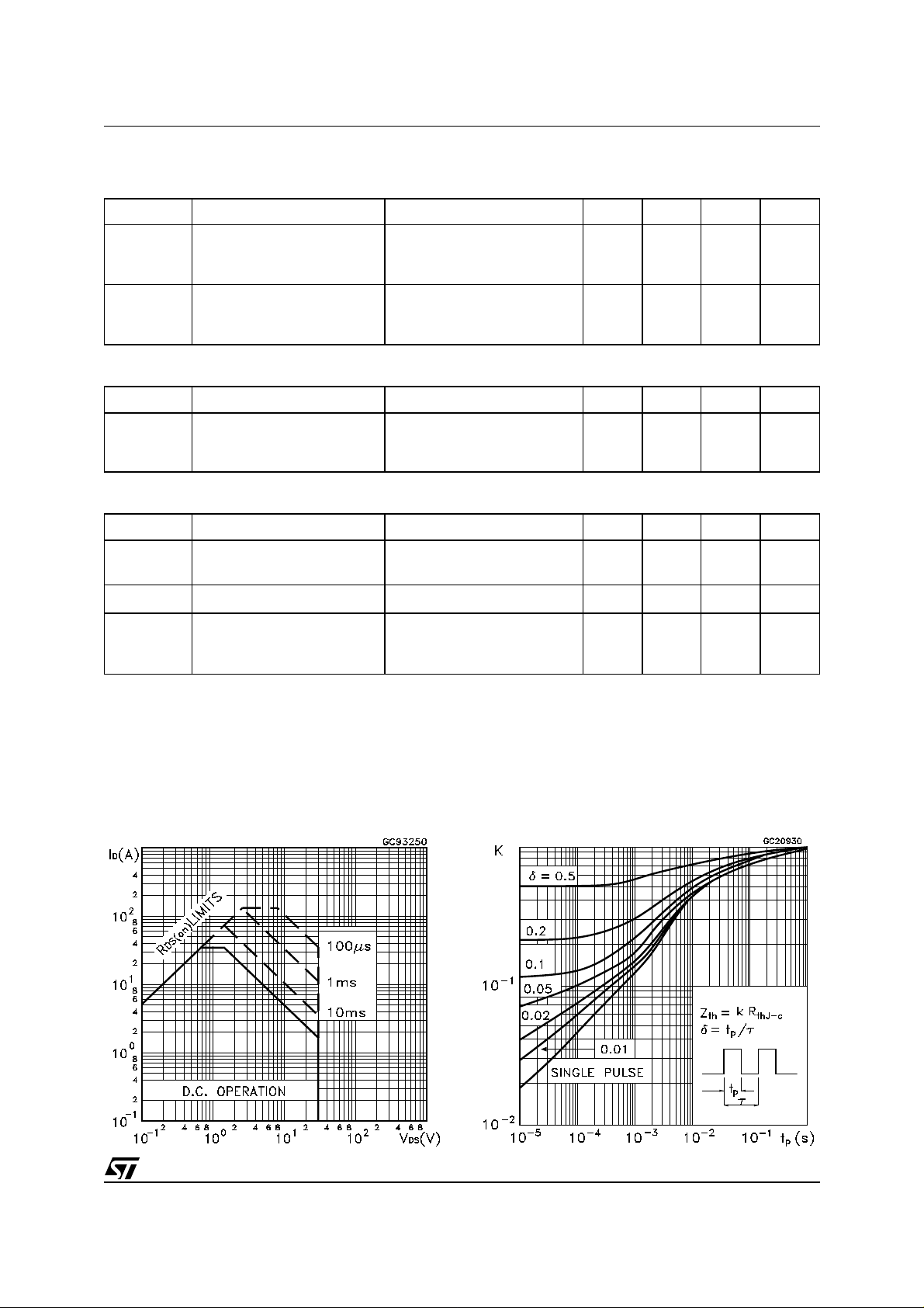
Safe Operating Area
Thermal Impedance
3/10
 Loading...