

SGS Thomson Microelectronics STD35NF06 Datasheet
STD35NF06
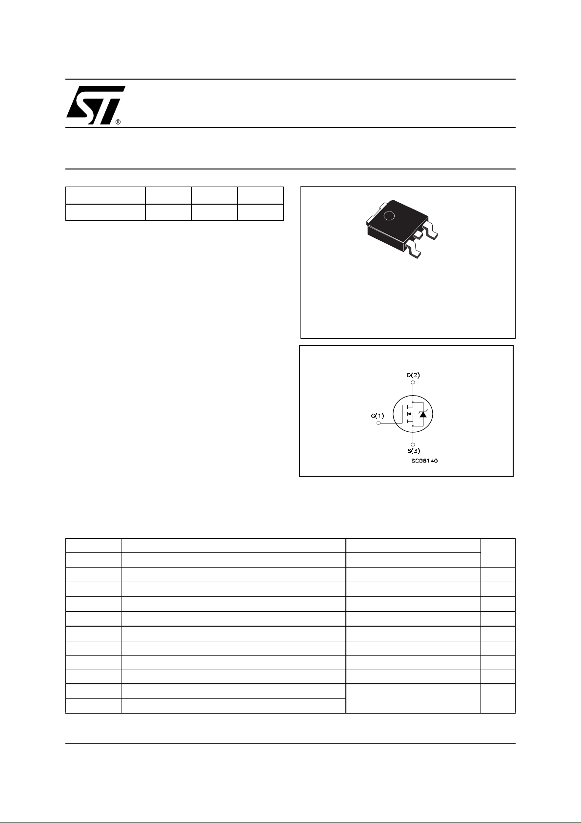
N-CHANNEL 60V - 0.018Ω - 35A DPAK
STripFET™II MOSFET
TYPE V
DSS
R
DS(on)
I
D
STD35NF06 60 V < 0.024 Ω 35 A
■ TYPICAL R
■ EXTREMELY HIGH dv /d t CAPABILITY
■ 100% AVALANCHE TESTED
■ GATE CHARGE MINIMIZED
(on) = 0.018 Ω
DS
DESCRIPTION
This Power Mosfet is the latest development of ST-
Microelectronics unique “Single Feature Size™”
strip-based process. The res ulting transistor sh ows
extremely high packing density for low on-resistance, rugged avalance characteristics and less critical alignment steps therefore a remarkable
manufacturing reproducibility.
APPLICATIONS
■ SOLENOID AND RELAY DRIVERS
■ MOTOR CONTROL, AUDIO AMPLIFIERS
■ DC-AC CONVERTERS
■ AUTOMOTIVE ENVIRONMENT
3
1
DPAK
INTERNAL SCHEMATIC DIAGRAM
ABSOLUTE MAXIMUM RATINGS
Symbol Parameter Value Unit
V
DS
V
DGR
V
GS
I
D
I
D
I
DM
P
TOT
dv/dt (1) Peak Diode Recovery voltage slope 5 V/ns
T
stg
T
j
(•)Pu l se width limi te d by safe oper at i ng area
Drain-source Voltage (VGS = 0)
Drain-gate Voltage (RGS = 20 kΩ)
60 V
60 V
Gate- source Voltage ± 20 V
Drain Current (continuos) at TC = 25°C
Drain Current (continuos) at TC = 100°C
(●)
Drain Current (pulsed) 140 A
Total Dissipation at TC = 25°C
35 A
24.5 A
55 W
Derating Factor 0.37 W/°C
Storage Temperature
Max. Operating Junction Temperature
(1)ISD ≤35A, di/dt ≤100A/µs, VDD ≤ V
–55 to 175 °C
, Tj ≤ T
(BR)DSS
JMAX.
1/9October 2001
STD35NF06
THERMA L D ATA
Rthj-case Thermal Resistance Junction-case Max 2.7 °C/W
Rthj-amb Thermal Resistance Junction-ambient Max 100 °C/W
T
l
AVALANCHE CHARACTERISTICS
Symbol Parameter Max Value Unit
I
AR
E
AS
ELECTRICAL CHARACTERISTICS (TCASE = 25 °C UNLESS OTHERWISE SPECIFIED)
OFF
Symbol Parameter Test Conditions Min. Typ. Max. Unit
V
(BR)DSS
I
DSS
I
GSS
Maximum Lead Temperature For Soldering Purpose 275 °C
Avalanche Current, Repetitive or Not-Repetitive
(pulse width limited by T
max)
j
Single Pulse Avalanche Energy
(starting T
Drain-source
= 25 °C, ID = IAR, VDD = 50 V)
j
ID = 250 µA, VGS = 0 60 V
17.5 A
130 mJ
Breakdown Voltage
Zero Gate Voltage
Drain Current (V
GS
Gate-body Leakage
Current (V
DS
= 0)
= 0)
V
= Max Rating
DS
V
= Max Rating, TC = 125 °C
DS
V
= ± 20V ±100 nA
GS
1µA
10 µA
ON
(1)
Symbol Parameter Test Conditions Min. Typ. Max. Unit
V
GS(th)
R
DS(on)
Gate Threshold Voltage
Static Drain-source On
V
= VGS, ID = 250µA
DS
VGS = 10V, ID = 17.5 A
234V
0.018 0.024 Ω
Resistance
DYNAMIC
Symbol Parameter Test Conditions Min. Typ. Max. Unit
(1) Forward Transconductance VDS > I
g
fs
C
iss
C
oss
C
rss
Input Capacitance
Output Capacitance 300 pF
Reverse Transfer
Capacitance
I
= 17.5 A
D
V
DS
D(on)
x R
DS(on)max,
= 25V, f = 1 MHz, VGS = 0
13 S
1530 pF
105 pF
2/9
STD35NF06
ELECTRICAL CHARACTERISTICS (CONTINUED)
SWITCHING ON
Symbol Parameter Test Conditions Min. Typ. Max. Unit
V
t
d(on)
Q
Q
Q
t
r
g
gs
gd
Turn-on Delay Time
Rise Time 8 ns
Total Gate Charge
Gate-Source Charge 10.5 nC
Gate-Drain Charge 17.5 nC
SWITCHING OFF
Symbol Parameter Test Conditions Min. Typ. Max. Unit
t
d(off)
t
f
Turn-off-Delay Time
Fall Time
SOURCE DRAIN DIODE
Symbol Parameter Test Conditions Min. Typ. Max. Unit
I
SD
I
SDM
VSD (1)
t
rr
Q
rr
I
RRM
Note: 1. Pulsed: Pu l se duration = 300 µs, duty c ycle 1.5 %.
2. Pulse width li mited by safe operating area.
Source-drain Current 35 A
(2)
Source-drain Current (pulsed) 140 A
Forward On Voltage
Reverse Recovery Time
Reverse Recovery Charge 170 nC
Reverse Recovery Current 4.5 A
= 30 V, ID = 27.5 A
DD
RG= 4.7Ω VGS = 10 V
(see test circuit, Figure 3)
V
= 48V, ID = 55 A,
DD
VGS = 10V
VDD = 30V, ID = 27.5A,
RG=4.7Ω, V
GS
= 10V
(see test circuit, Figure 3)
ISD = 35 A, VGS = 0
I
= 35 A, di/dt = 100A/µs
SD
VDD = 20V, Tj = 150°C
(see test circuit, Figure 5)
16 ns
44.5 60 nC
36
15
1.5 V
75 ns
ns
ns
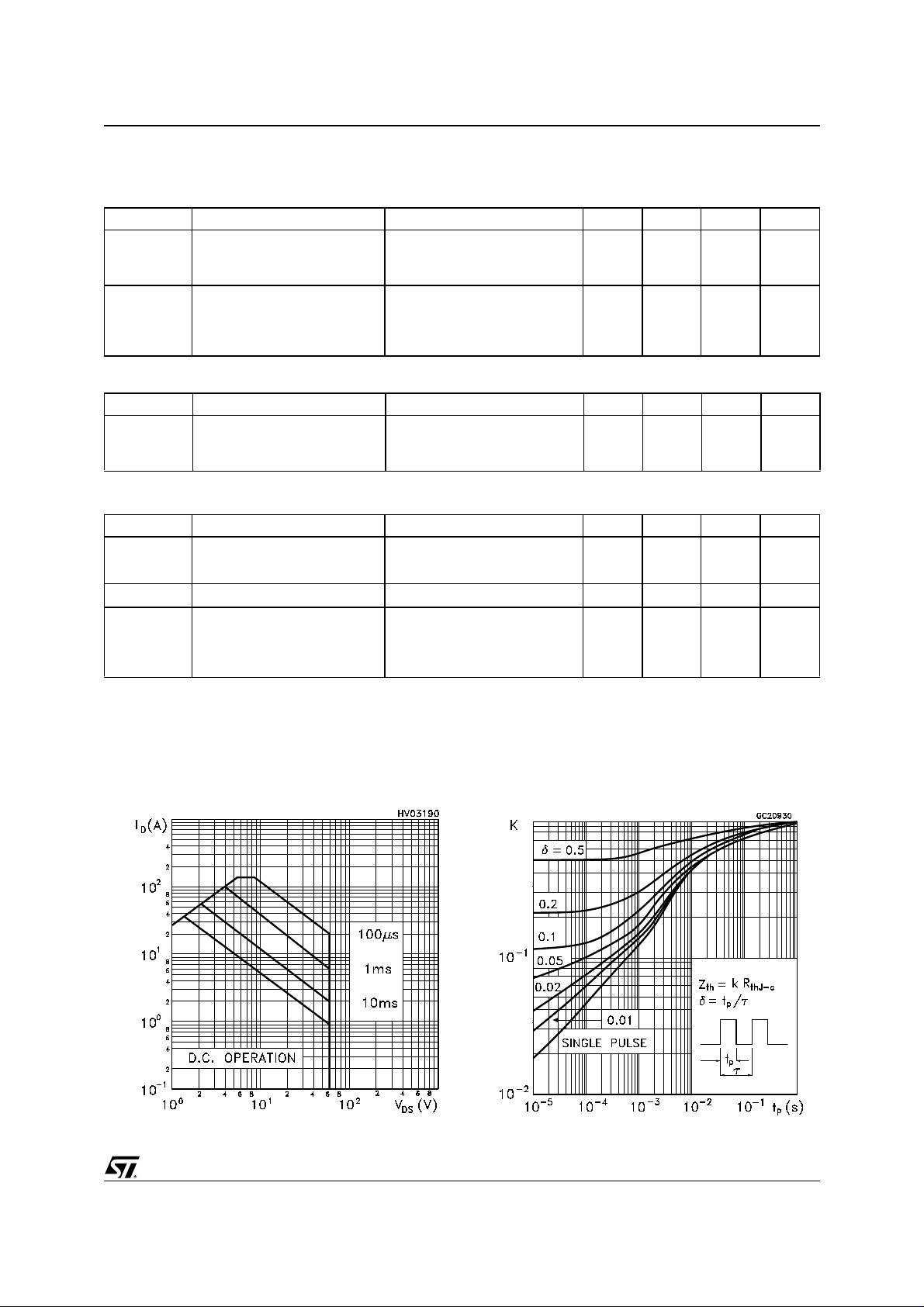
Safe Operating Area
Thermal Imp e dence
3/9
 Loading...