

SGS Thomson Microelectronics STD30PF03L, STD30PF03L-1 Datasheet
STD30PF03L
STD30PF03L-1
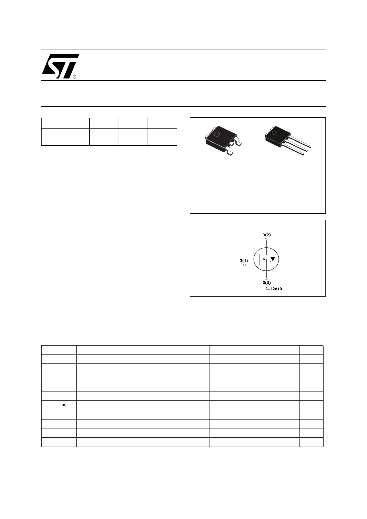
P-CHANNEL 30V - 0.025Ω - 24A DPAK/IPAK
STripFET™ II POWER MOSFET
PRELIMINARY DATA
TYPE V
STD30PF03 L
STD30PF03 L-1
■ TYPICAL R
■ STANDARD OUTLI N E FOR EAS Y
DS(on)
DSS
30 V
30 V
= 0.025Ω
R
DS(on)
< 0.028Ω
< 0.028Ω
I
D
24 A
24 A
AUTOMATED SURFACE MOUNT ASSEMBLY
■ LOW THRESHOLD DRIVE
■ LOW GATE CHARGE
■ EXTREMELY LOW FIGURE OF MERIT
(R
DS(on) * Qg
)
DESCRIPTION
This Power MOSFET is the latest dev elo pment of
STMicroelectronics unique “Single Feature
Size™” strip-based process. The resulting transistor shows extremely high packing density for low
on-resistance and low gate charge.
APPLICATIONS
■ DC-DC CONVERTERS
3
DPAK
1
IPAK
1
INTERNAL SCHEMATIC DIAGRAM
3
2
ABSOLUTE MAXIMUM RATINGS
Symbol Parameter Value Unit
V
DS
V
DGR
V
GS
I
(#) Drain Current (continuous) at TC = 25°C
D
ID (#) Drain Current (continuous) at TC = 100°C
I
DM
P
TOT
T
stg
T
j
(●) Pulse width limited by safe operating area
(#) Curre nt lim i ted by wire bonding
May 2002
Drain-source Voltage (VGS = 0)
Drain-gate Voltage (RGS = 20 kΩ)
Gate- source Voltage ± 16 V
(l)
Drain Current (pulsed) 96 A
Total Dissipation at TC = 25°C
Derating Factor 0.47 W/°C
Storage Temperature – 55 to 175 °C
Max. Operating Junction Temperature 175 °C
Note:For the P-CHANNEL MOSFET actual polarity of voltages and
30 V
30 V
24 A
24 A
70 W
current has to be reve rsed
1/8
STD30PF03L - STD30PF03L-1
THERMA L D ATA
Rthj-case Thermal Resistance Junction-case Max 2.14 °C/W
Rthj-amb Thermal Resistance Junction-ambient Max 100 °C/W
T
j
AVALANCHE CHARACTERISTICS
Symbol Parameter Max Value Unit
I
AR
E
AS
ELECTRICAL CHARACTERISTICS (TCASE = 25 °C UNLESS OTHERWISE SPECIFIED)
OFF
Symbol Parameter Test Conditions Min. Typ. Max. Unit
V
(BR)DSS
I
DSS
I
GSS
Maximum Operating Junction Temperature 275 °C
Avalanche Current, Repetitive or Not-Repetitive
(pulse width limited by T
max)
j
Single Pulse Avalanche Energy
(starting T
Drain-source
= 25 °C, ID = IAR, VDD = 25 V)
j
ID = 250 µA, VGS = 0 30 V
24 A
350 mJ
Breakdown Voltage
Zero Gate Voltage
Drain Current (V
GS
Gate-body Leakage
Current (V
DS
= 0)
= 0)
V
= Max Rating
DS
V
= Max Rating, TC = 125 °C
DS
V
= ± 16 V ±100 nA
GS
1µA
10 µA
ON
(1)
Symbol Parameter Test Conditions Min. Typ. Max. Unit
V
GS(th)
R
DS(on)
Gate Threshold Voltage
Static Drain-source On
Resistance
V
= VGS, ID = 250µA
DS
VGS = 10 V, ID = 12 A
VGS = 5 V, ID = 12 A
1V
0025 0.028 Ω
0.032 0.040 Ω
DYNAMIC
Symbol Parameter Test Conditions Min. Typ. Max. Unit
(1) Forward Transconductance VDS = 15 V, ID= 12 A 23 S
g
fs
C
iss
C
oss
C
rss
Input Capacitance
Output Capacitance 345 pF
Reverse Transfer
Capacitance
V
= 25V, f = 1 MHz, VGS = 0
DS
1670 pF
120 pF
2/8
STD30PF03L - STD30PF03L-1
ELECTRICAL CHARACTERISTICS (CONTINUED)
SWITCHING ON
Symbol Parameter Test Conditions Min. Typ. Max. Unit
V
t
d(on)
Q
Q
Q
t
r
g
gs
gd
Turn-on Delay Time
Rise Time 122 ns
Total Gate Charge
Gate-Source Charge
Gate-Drain Charge
SWITCHING OFF
Symbol Parameter Test Conditions Min. Typ. Max. Unit
t
d(off)
t
f
Turn-off-Delay Time
Fall Time
SOURCE DRAIN DIODE
Symbol Parameter Test Conditions Min. Typ. Max. Unit
I
SD
I
SDM
VSD (1)
t
rr
Q
rr
I
RRM
Note: 1. Pulsed: Pu l se duration = 300 µs, duty c yc l e 1.5 %.
2. Pulse width li mited by safe operating area.
Source-drain Current 24 A
(2)
Source-drain Current (pulsed) 96 A
Forward On Voltage
Reverse Recovery Time
Reverse Recovery Charge
Reverse Recovery Current
= 24 V, ID = 24 A
DD
R
= 4.7Ω VGS = 4.5V
G
(see test circuit, Figure 3)
VDD = 15 V, ID = 24 A,
VGS = 5 V
VDD = 24 V, ID = 24 A,
RG=4.7Ω, V
GS
= 4.5V
(see test circuit, Figure 3)
ISD = 24 A, VGS = 0
= 24 A, di/dt = 100 A/µs,
I
SD
VDD = 24 V, Tj = 150 °C
(see test circuit, Figure 5)
64 ns
18.5
25 nC
5.5
11
36
26
2.3 V
40
52
2.6
nC
nC
ns
ns
ns
µC
A
3/8
 Loading...