

SGS Thomson Microelectronics STD30NF03L Datasheet
STD30NF03L
N - CHANNEL 30V - 0.020 Ω - 30A DPAK
STripFET POWER MOSFET
TYPE V
DSS
R
DS(o n)
I
D
ST D30N F 03L 30 V < 0.025 Ω 30 A
■ TYPICALR
■ LOW THRESHOLDDRIVE
■ ADDSUFFIX ”T4” FORORDERING INTAPE
DS(on)
= 0.020 Ω
& REEL
DESCRIPTION
This PowerMOSFET is the latest developmentof
STMicroelectronics unique ”Single Feature
Size” strip-based process. The resulting
transistor shows extremely high packing density
for low on-resistance, rugged avalanche
characteristics and less critical alignment steps
therefore a remarkable manufacturing
reproducibility.
APPLICATIONS
■ HIGHCURRENT, HIGH SPEED SWITCHING
■ SOLENOIDAND RELAYDRIVERS
■ MOTORCONTROL, AUDIO AMPLIFIERS
■ DC-DC& DC-ACCONVERTERS
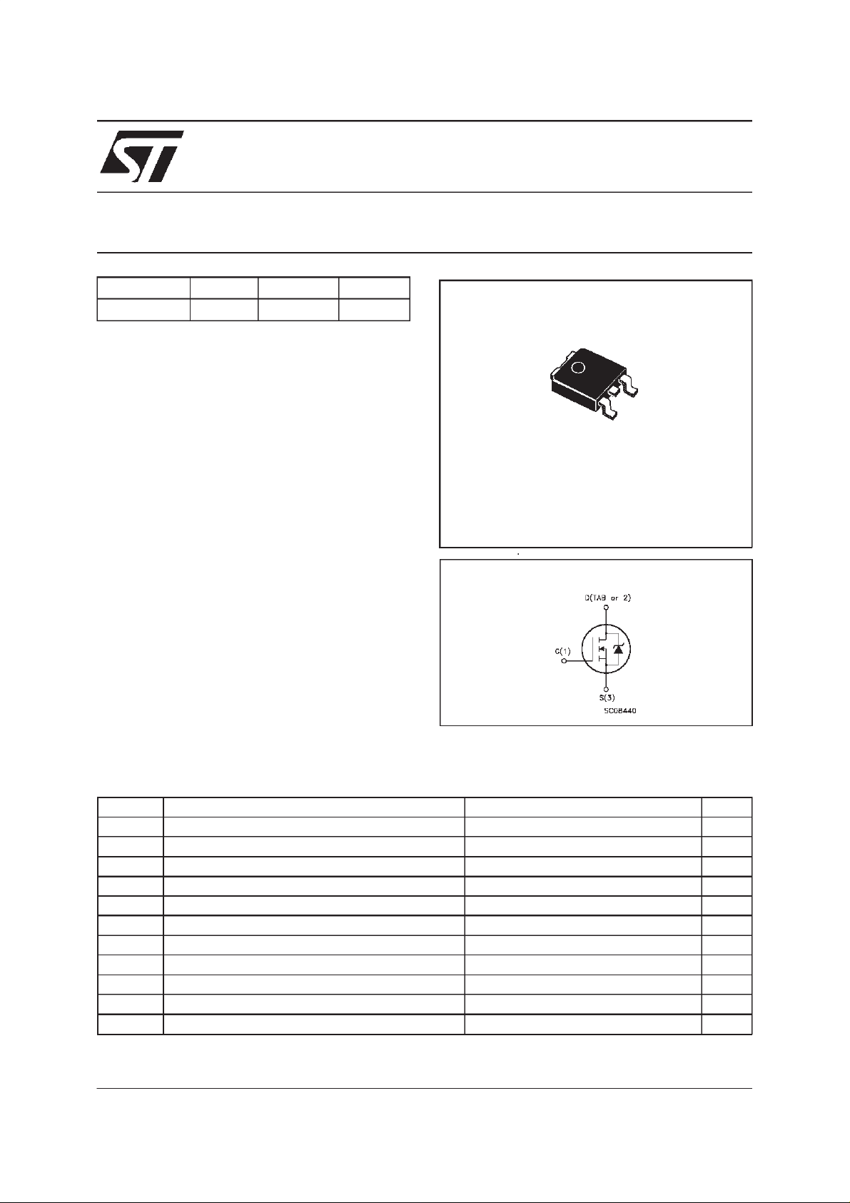
3
1
DPAK
TO-252
(Suffix ”T4”)
INTERNAL SCHEMATIC DIAGRAM
ABSOLUTE MAXIMUM RATINGS
Symbol Parameter Value Uni t
V
V
V
I
D
I
DM
P
E
AS
T
(••) Pulse width limitedby safe operating area (1) starting Tj
(•)Currentlimitedby the package
October 1999
Dra in- sour c e Vol ta ge (VGS=0) 30 V
DS
Drain- gate Voltage (RGS=20kΩ)30V
DGR
Gate-s ource Volt age ± 20 V
GS
(•) Dra in Current (conti nuous ) at Tc=25oC30A
Dra in Current (conti nuous) at Tc= 100oC19A
I
D
(
Dra in Current (pulsed) 120 A
••)
Tot al Dissi pat io n at Tc=25oC40W
tot
Der ati ng Fact or 0.27 W/
o
C
(1) Single Pulse Avalanche Energy 100 m/ J
St orage Tem pe ra t ure -65 to 175
stg
Max. Operat ing Junct ion Tempera t ure 175
T
j
=25oC,ID=15A, VDD= 15V
o
C
o
C
1/8

STD30NF03L
THERMAL DATA
R
thj-pcb
R
thj-amb
R
thj-sink
T
Ther mal Resistanc e Junct ion-PC Boa rd Max
Ther mal Resistanc e Junct ion-ambient Max
Ther mal Resistanc e Case-sink Ty p
Maximum Lead Te m perature F or S o lder ing Purpose
l
3.75
100
1.5
275
o
C/W
o
C/W
o
C/W
o
C
ELECTRICAL CHARACTERISTICS
=25oC unless otherwisespecified)
(T
case
OFF
Symbol Parameter Test Conditions Min. Typ. Max. Unit
V
(BR)DSS
Drain-source
ID=250µAVGS=0 30 V
Break dow n Voltage
I
DSS
I
GSS
Zero Gate Voltage
Drain Current (V
GS
Gat e- bod y Leakage
Current (V
DS
=0)
=0)
V
=MaxRating
DS
=MaxRating Tc= 125oC
V
DS
V
= ± 20 V ± 100 nA
GS
1
10
ON(∗)
Symbol Parameter Test Conditions Min. Typ. Max. Unit
V
GS(th)
R
DS(on)
I
D(on)
Gate Threshold Volt age VDS=VGSID= 250 µ A11.72.5V
Sta t ic Drain-sour ce On
Resistance
VGS=10V ID=15A
=4.5V ID=15A
V
GS
On State Drain Current VDS>I
D(on)xRDS(on )max
0.020
0.028
30 A
0.025
0.035ΩΩ
VGS=10V
DYNAMIC
Symbol Parameter Test Conditions Min. Typ. Max. Unit
g
(∗)Forward
fs
Tr ansc on duc tance
C
C
C
Input Capacitance
iss
Out put Capacitance
oss
Reverse Transfer
rss
Capacit a nc e
VDS>I
D(on)xRDS(on )maxID
=15A 13 S
VDS=25V f=1MHz VGS= 0 V 830
230
92
µ
µA
pF
pF
pF
A
2/8
STD30NF03L
ELECTRICAL CHARACTERISTICS
(continued)
SWITCHING ON
Symbol Parameter Test Conditions Min. Typ. Max. Unit
t
d(on)
Tur n-on Delay Time
Rise Time
t
r
VDD=15V ID=20A
R
=4.7
G
Ω
VGS=4.5V
35
205
(Resis t iv e Load, see fig. 3)
Q
Q
Q
Tot al Gate Charge
g
Gat e- Source Char g e
gs
Gate-Drain Charge
gd
VDD=24V ID=30A VGS=5V 18
7
8
SWITCHING OFF
Symbol Parameter Test Conditions Min. Typ. Max. Unit
t
d(off)
Tur n-of f Delay Time
t
Fall T ime
f
VDD=15V ID=20A
=4.7 Ω VGS=4.5V
R
G
90
240
(Resis t iv e Load, see fig. 3)
SOURCEDRAIN DIODE
Symbol Parameter Test Conditions Min. Typ. Max. Unit
I
V
I
SDM
SD
Q
I
RRM
SD
t
Source-drain Current
(•)
Source-drain Current
30
120
(pulsed)
(∗)ForwardOnVoltage ISD=30A VGS=0 1.5 V
Reverse Recovery
rr
Time
Reverse Recovery
rr
ISD= 40 A di/dt = 100 A/µs
=15V Tj=150oC
V
DD
(see test circuit, fig. 5)
65
72
Charge
Reverse Recovery
2
Current
ns
ns
nC
nC
nC
ns
ns
A
A
ns
nC
A
(∗) Pulsed: Pulse duration= 300µs, dutycycle 1.5 %
(•) Pulse width limited by safeoperating area
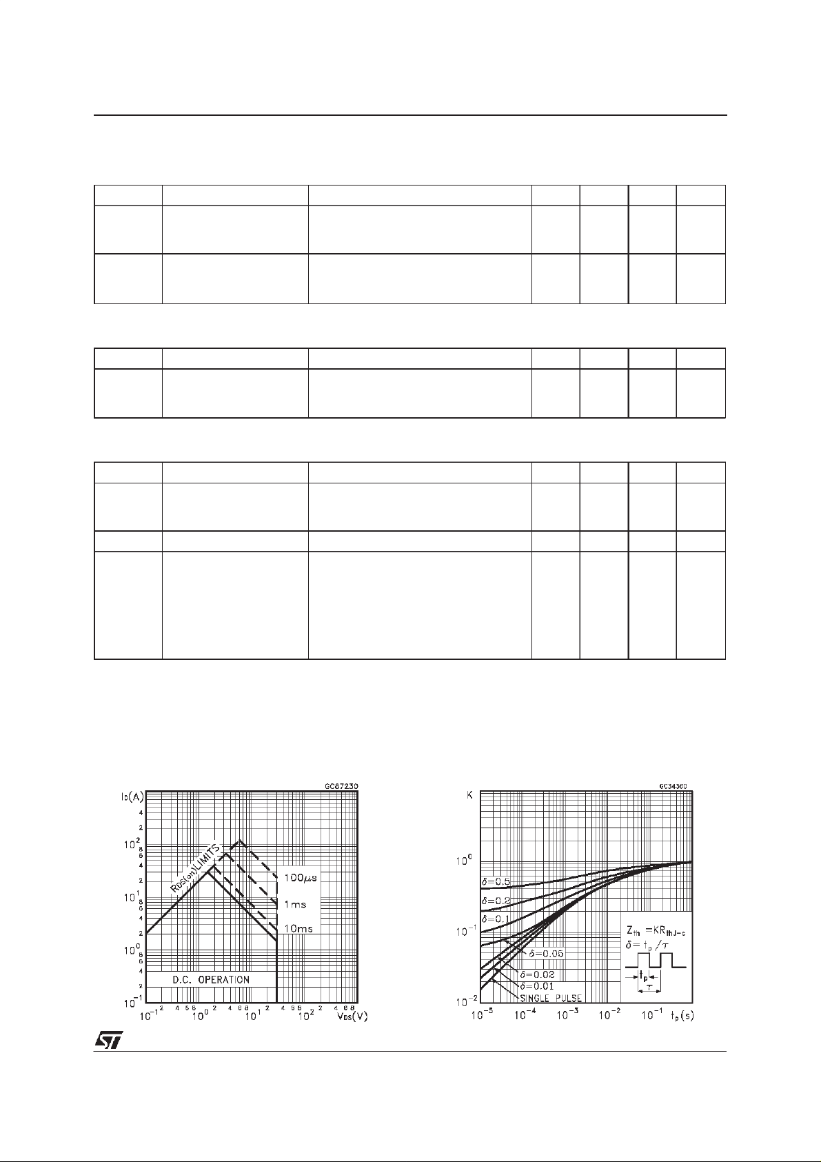
SafeOperating Area ThermalImpedance
3/8
 Loading...