

SGS Thomson Microelectronics STQ1NC45R, STD2NC45-1 Datasheet
1/11June 2003
STD2NC45-1
STQ1NC45
N-CHANNEL 450V - 4.1Ω - 1 .5 A IPAK / TO-92
SuperMESH™Power MOSFET
■ TYPICAL R
DS
(on) = 4.1 Ω
■ EXTREMELY HIGHdv/dt CAPABILITY
■ 100% AVALANCHE TESTED
■ GATE CHARGE MINIMIZED
■ NEW HIGH VOLTAGE BENCHMARK
DESCRIPTION
The SuperMESH™ series is obtained through an
extreme optimization of ST’s we ll established stripbased PowerMESH™ layout. In addition to pushing
on-resistance significantly down, special careis taken to ensure a very good dv/dt capability for the
most demanding applications. Such series complements ST full range of high voltage MOSFETs including revolutionary MDm es h™ products.
APPLICATIONS
■ SWITCH MODE LOW POWER SUPPLIES
(SMPS)
■ LOW POWER, LOW COST CFL (COMPACT
FLUORESCENT LAMPS)
■ LOW POWER BATTERY CHARGERS
ORDERING INFORMATION
TYPE V
DSS
R
DS(on)
I
D
Pw
STD2NC45-1
STQ1NC45
450 V
450 V
< 4.5 Ω
< 4.5 Ω
1.5 A
0.5 A
30 W
3.1 W
SALES TYPE MARKING PACKAGE PACKAGING
STD2NC45-1 D2NC45 IPAK TUBE
STQ1NC45 Q1NC45 TO-92 BULK
STQ1NC45-AP Q1NC45 TO-92 AMMOPAK
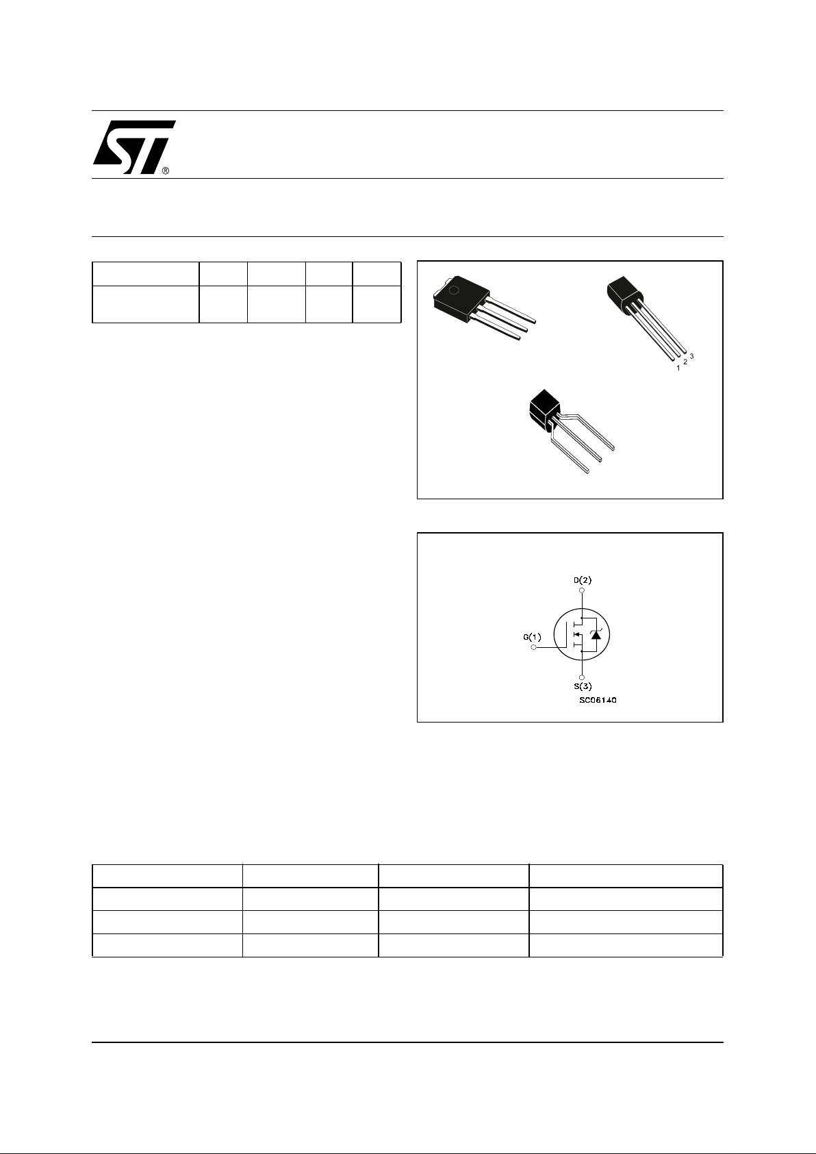
IPAK
3
2
1
TO-92
TO-92 (Ammopack)
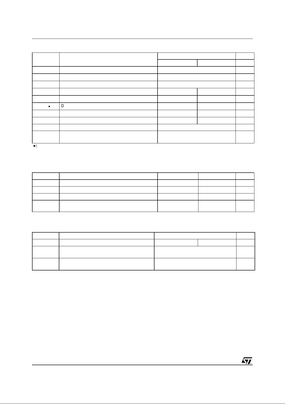
INTERNAL SCHEMATIC DIAGRAM
STD2NC45-1, STQ1NC45
2/11
ABSOLUTE MAXIMUM RATINGS
() Pulse width limited by safe operating area
(1) I
SD
≤0.5A, di/dt ≤100A/µs, VDD≤ V
(BR)DSS,Tj≤TJMAX.
THERMAL DATA
AVALANCHE CHARACTERISTICS
Symbol Parameter Value Unit
STD2NC45-1 STQ1NC45
V
DS
Drain-source Voltage (VGS=0)
450 V
V
DGR
Drain-gate Voltage (RGS=20kΩ)
450 V
V
GS
Gate- source Voltage ± 30 V
I
D
Drain Current (continuos) at TC= 25°C
1.5 0.5 A
I
D
Drain Current (continuos) at TC= 100°C
0.95 0.315 A
IDM()
Drain Current (pulsed) 6 2 A
P
TOT
Total Dissipation at TC= 25°C
30 3.1 W
Derating Factor 0.24 0.025 W/°C
dv/dt (1) Peak Diode Recovery voltage slope 3 V/ns
T
j
T
stg
Operating Junction Temperature
Storage Temperature
-65 to 150
-65 to 150
°C
°C
IPAK TO-92
Rthj-case Thermal Resistance Junction-case Max 4.1 °C/W
Rthj-amb Thermal Resistance Junction-ambient Max 100 120 °C/W
Rthj-lead Thermal Resistance Junction-lead Max 40 °C/W
T
l
Maximum Lead Temperature For Soldering
Purpose
275 260 °C
Symbol Parameter Max Value Unit
IPAK TO-92
I
AR
Avalanche Current, Repetitive or Not-Repetitive
(pulse width limited by T
j
max)
1.5 A
E
AS
Single Pulse Avalanche Energy
(starting T
j
= 25 °C, ID=IAR,VDD=50V)
25 mJ
3/11
STD2NC45-1, STQ1NC45
ELECTRICAL CHARACTERISTICS (TCASE =25°C UNLESS OT HERWISE SPECIFIED)
ON/OFF
DYNAMIC
SWITCHING ON
SWITCHING OFF
SOURCE DRAIN DIODE
Note: 1. Pulsed: Pulse duration = 300 µs, duty cycle 1.5 %.
2. Pulse width limited by safe operating area.
Symbol Parameter Test Conditions Min. Typ. Max. Unit
V
(BR)DSS
Drain-source
Breakdown Voltage
ID= 250 µA, VGS= 0 450 V
I
DSS
Zero Gate Voltage
Drain Current (V
GS
=0)
V
DS
= Max Rating
VDS= Max Rating, TC= 125 °C
1
50
µA
µA
I
GSS
Gate-body Leakage
Current (V
DS
=0)
V
GS
= ± 30V ±100 nA
V
GS(th)
Gate Threshold Voltage
V
DS=VGS,ID
= 250µA
2.3 3 3.7 V
R
DS(on)
Static Drain-source On
Resistance
VGS=10V,ID= 0.5 A 4.1 4.5 Ω
Symbol Parameter Test Conditions Min. Typ. Max. Unit
g
fs
(1) Forward Transconductance VDS>I
D(on)xRDS(on)max,
ID= 0.5 A
1.1 S
C
iss
C
oss
C
rss
Input Capacitance
Output Capacitance
Reverse Transfer
Capacitance
V
DS
=25V,f=1MHz,VGS=0
160
27.5
4.7
pF
pF
pF
Symbol Parameter Test Conditions Min. Typ. Max. Unit
t
d(on)
t
r
Turn-on Delay Time
Rise Time
VDD=225V,ID= 0.5 A
R
G
= 4.7Ω VGS=10V
(Resistive Load see, Figure 3)
6.7
4
ns
ns
Q
g
Q
gs
Q
gd
Total Gate Charge
Gate-Source Charge
Gate-Drain Charge
V
DD
=360V,ID= 1.5 A,
VGS=10V,RG= 4.7Ω
7
1.3
3.2
10
nC
nC
nC
Symbol Parameter Test Conditions Min. Typ. Max. Unit
t
r(Voff)
t
f
t
c
Off-voltage Rise Time
Fall Time
Cross-over Time
V
DD
= 360V, ID= 1.5 A,
R
G
=4.7Ω, VGS= 10V
(Inductive Load see, Figure 5)
8.5
12
18
ns
ns
ns
Symbol Parameter Test Conditions Min. Typ. Max. Unit
I
SD
I
SDM
(2)
Source-drain Current
Source-drain Current (pulsed)
1.5
6.0
A
A
V
SD
(1)
Forward On Voltage
ISD= 1.5 A, VGS=0
1.6 V
t
rr
Q
rr
I
RRM
Reverse Recovery Time
Reverse Recovery Charge
Reverse Recovery Current
I
SD
= 1.5 A, di/dt = 100A/µs
VDD=100V,Tj=150°C
(see test circuit, Figure 5)
225
530
4.7
ns
µC
A
STD2NC45-1, STQ1NC45
4/11
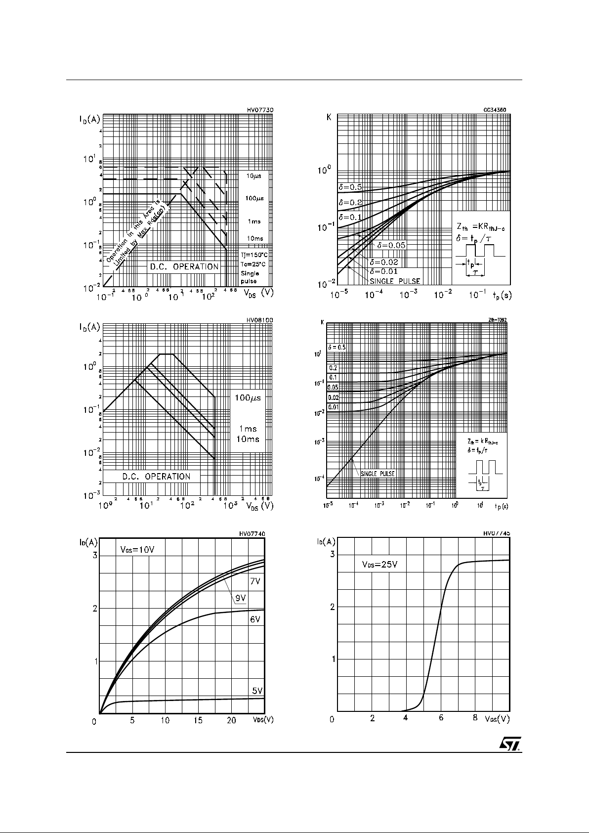
Safe Operating Area For IPAK
Thermal Impedance For TO-92Safe Operating Area For TO-92
Thermal Imped ance For IPAK
Output Characteristics
Transfer Characteristics
 Loading...