

SGS Thomson Microelectronics STD2NB60-1, STD2NB60T4 Datasheet
STD2NB60
N - CHANNEL ENHANCEMENT MODE
PowerMESH MOSFET
TYPE V
DSS
R
DS(on)
I
D
STD2NB60 600 V < 3.6 Ω 2.6 A
■ TYPICAL R
■ EXTREM E LY HIG H dv/ dt CA P A BILIT Y
■ 100% AVALANCHE TESTED
■ VERY LOW INTRINSIC CAPACITANCES
■ GATE CHARGE MINIMIZED
DS(on)
= 3.3 Ω
DESCRIPTION
Using the latest high voltage MESH OVERLAY
process, SGS-Thomson has designed an
advanced family of power MOSFETs with
outstanding performances. The new patent
pending strip layout coupled with the Company’s
proprietary edge termination structure, gives the
lowest R
per area, exceptional avalanche
DS(on)
and dv/dt capabilities and unrivalled gate charge
and switching char acteristics.
APPLICATIONS
■ SWITCH MODE POWE R SUPPLI ES (SMPS)
■ DC-AC CONVE RTERS FOR WELDI NG
EQUIPMENT AND UNINTERRUPTIBLE
POWER SUPPLIES AND MOTOR DRIVE
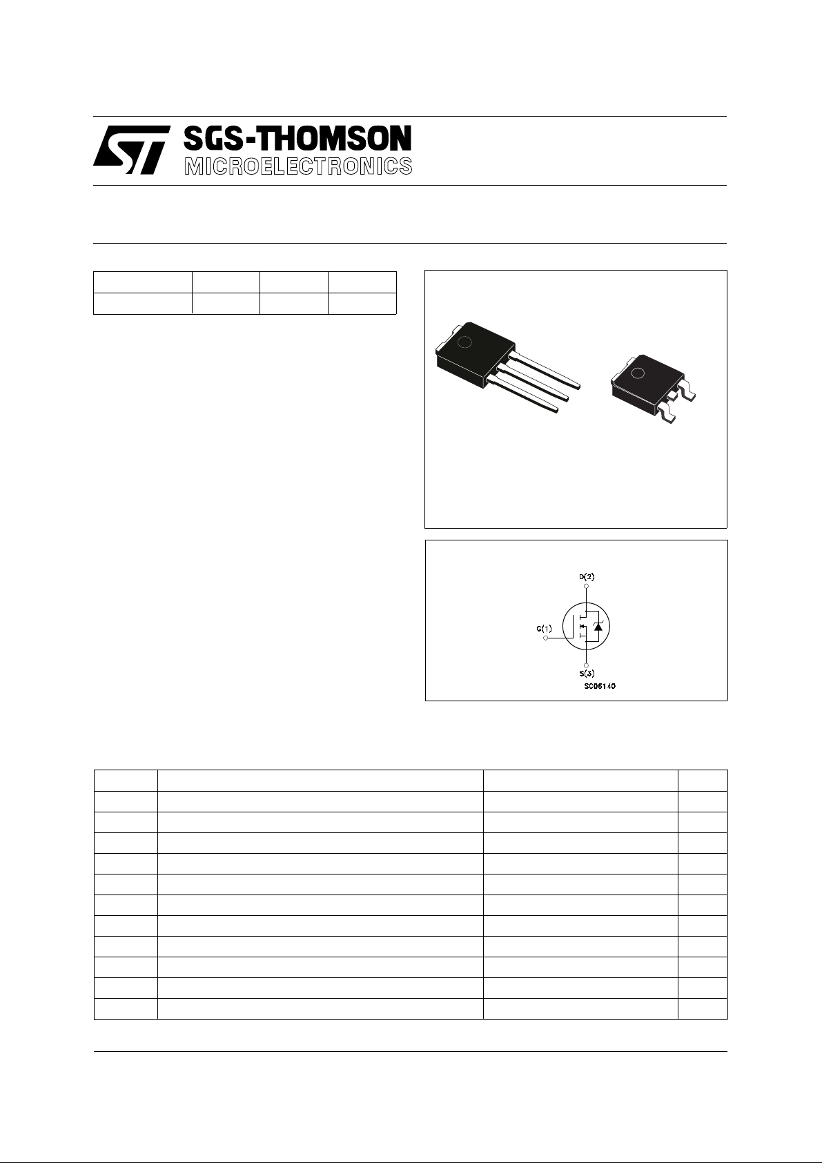
3
2
IPAK
TO-251
(Suffix "- 1")
1
(Suffix "T4")
1
DPAK
TO-252
INTER NAL SCH E M ATI C DIAG RA M
3
ABSOLUTE MAXIMUM RATINGS
Symbol Parameter Value Unit
V
V
V
IDM(•) Drain Current (pulsed) 10.4 A
P
dv/dt(1) Peak Diode Recovery voltage slope 4.5 V/ns
T
(•) Pulse width limited by safe operating area (1) ISD ≤2.6A, di/dt ≤ 200 A/µs, VDD ≤ V
March 1998
Drain-source Voltage (VGS = 0) 600 V
DS
Drain- gate Voltage (RGS = 20 kΩ)
DGR
Gate-source Voltage ± 30 V
GS
I
Drain Current (continuous) at Tc = 25 oC 2.6 A
D
I
Drain Current (continuous) at Tc = 100 oC 1.6 A
D
Total Dissipation at Tc = 25 oC50W
tot
600 V
Derating Factor 0.4 W/
Storage Temperature -65 to 150
stg
T
Max. Operating Junction Temperature 150
j
, Tj ≤ T
(BR)DSS
JMAX
o
C
o
C
o
C
1/9
STD2NB60
THERMAL DATA
R
thj-case
Rthj-amb
R
thc-si n k
T
Thermal Resistance Junction-case Max
Thermal Resistance Junction-ambient Max
Thermal Resistance Case-sink Typ
Maximum Lead Temperature For Soldering Purpose
l
AVALANCHE CHARACTERI S TICS
Symbol Parameter Max Value Unit
I
AR
E
Avalanche Current, Repetitive or Not-Repetitive
(pulse width limited by T
Single Pulse Avalanche Energy
AS
(starting T
= 25 oC, ID = IAR, V
j
ma x, δ < 1%)
j
DD
= 50 V)
2.5
100
1.5
275
2.6 A
80 mJ
o
C/W
oC/W
o
C/W
o
C
ELECTRICAL CHARACTERISTICS (T
= 25 oC unless otherwise specified)
case
OFF
Symbol Parameter Test Conditions Min. Typ. Max. Unit
V
(BR)DSS
Drain-source
I
= 250 µA V
D
GS
= 0
600 V
Breakdown Voltage
I
DSS
I
GSS
Zero Gate Voltage
Drain Current (V
GS
Gate-body Leakage
Current (V
DS
= 0)
= 0)
= Max Rating
V
DS
V
= Max Rating Tc = 125 oC
DS
V
= ± 30 V
GS
1
50
± 100 nA
ON (∗)
Symbol Parameter Test Conditions Min. Typ. Max. Unit
V
GS(th)
Gate Threshold
V
= VGS ID = 250 µA
DS
345V
Voltage
R
DS(on)
Static Drain-source On
VGS = 10V ID =1.6 A 3.3 3.6 Ω
Resistance
I
D(on)
On State Drain Current VDS > I
V
= 10 V
GS
D(on)
x R
DS(on)max
3.3 A
DYNAMIC
Symbol Parameter Test Conditions Min. Typ. Max. Unit
g
(∗) Forward
fs
Transconductance
C
C
C
Input Capacitance
iss
Output Capacitance
oss
Reverse Transfer
rss
Capacitance
VDS > I
V
DS
x R
D(on)
DS(on)max
= 25 V f = 1 MHz V
ID = 1.6 A 1.2 2 S
= 0 400
GS
57
520
77
7
9
µA
µA
pF
pF
pF
2/9
STD2NB60
ELECTRICAL CHARACTERISTICS (continued)
SWITCHING O N
Symbol Parameter Test Conditions Min. Typ. Max. Unit
t
d(on)
t
Q
Q
Q
SWITCHING O F F
Symbol Parameter Test Conditions Min. Typ. Max. Unit
t
r(Voff)
t
SOURCE DRAIN DIO DE
Symbol Parameter Test Conditions Min. Typ. Max. Unit
I
SD
I
SDM
V
SD
t
Q
I
RRM
(∗) Pulsed: Pulse duration = 300 µs, duty cycle 1.5 %
(•) Pulse width limited by safe operating area
r
Turn-on Time
Rise Time
V
= 300 V ID = 1.6 A
DD
RG = 4.7 Ω VGS = 10 V
11
17
7
11
(see test circuit, figure 3)
Total Gate Charge
g
Gate-Source Charge
gs
Gate-Drain Charge
gd
Off-voltage Rise Time
Fall Time
t
f
Cross-over Time
c
Source-drain Current
(•)
Source-drain Current
V
= 480 V ID =3.3 A V
DD
V
= 480 V ID = 3.3 A
DD
= 4.7 Ω VGS = 10 V
R
G
(see test circuit, figure 5)
= 10 V 15
GS
6.2
5.6
11
13
18
22 nC
16
18
25
3.3
13.2
(pulsed)
(∗) Forward On Voltage ISD = 3.3 A VGS = 0 1.6 V
Reverse Recovery
rr
Time
Reverse Recovery
rr
I
= 3.3 A di/dt = 100 A/µs
SD
V
= 100 V Tj = 150 oC
DD
(see test circuit, figure 5)
500
2.1
Charge
Reverse Recovery
8.5
Current
ns
ns
nC
nC
ns
ns
ns
A
A
ns
µC
A
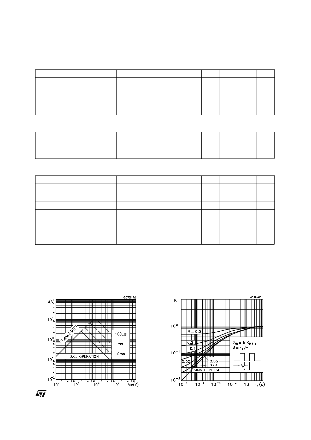
Safe Operating Are a Thermal Impe dance
3/9
 Loading...