

SGS Thomson Microelectronics STD2NB50, STD2NB50-1 Datasheet
STD2NB50
3
STD2NB50-1
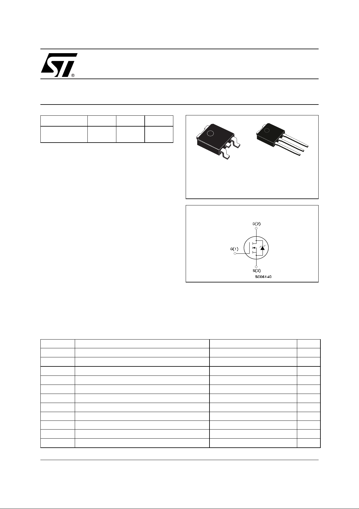
N-CHANNEL 500V - 5Ω - 1A DPAK / IPAK
PowerMesh™ MOSFET
TYPE V
STD2NB50
STD2NB50-1
■ TYPICAL R
■ 100% AVALANCHE TESTED
■ VERY LOW INTRINSIC CAPAC ITANCES
■ ADD SUFFIX “T4” FOR ORDERING IN TAPE &
DS
DSS
500V
500V
(on) = 5 Ω
R
DS(on)
< 6Ω
< 6Ω
I
D
1 A
1 A
REEL
DESCRIPTION
Using the latest high voltage MESH OVERLAY™
process, STMicroelectronics has designed an advanced family of power MOSFETs with outstanding
performances. The new patent pending strip layout
coupled with the Company’s proprieraty edge termination structure, gives the lowest RDS(on) per area,
exceptional avalanche and dv/dt capabilities and
unrivalled gate charge and switching characteristics.
APPLICATIONS
■ SWITH MODE POWER SUPPLI ES ( SMPS)
■ LIGHTING FOR INDUSTRIAL AND CONSUMER
ENVIRONMENT
3
1
DPAK IPAK
INTERNAL SCHEMATIC DIAGRAM
2
1
ABSOLUTE MAXIMUM RATINGS
Symbol Parameter Value Unit
V
DS
V
DGR
V
GS
I
D
I
D
I
DM
P
TOT
dv/dt(1) Peak Diode Recovery voltage slope 3.5 V/ns
T
stg
T
j
(•)Pu l se width limited by safe operating area
Drain-source Voltage (VGS = 0)
Drain-gate Voltage (RGS = 20 kΩ)
Gate- source Voltage ± 30 V
Drain Current (continuos) at TC = 25°C
Drain Current (continuos) at TC = 100°C
(●)
Drain Current (pulsed) 4 A
Total Dissipation at TC = 25°C
Derating Factor 0.32 W/°C
Storage Temperature –65 to 150 °C
Max. Operating Junction Temperature 150 °C
(1)ISD ≤1A, di/dt ≤200A/µs, VDD ≤ V
500 V
500 V
1A
0.63 A
40 W
, Tj ≤ T
(BR)DSS
JMAX.
1/10September 2001
STD2NB50/STD2NB50-1
THERMA L D ATA
Rthj-case Thermal Resistance Junction-case Max 3.125 °C/W
Rthj-amb Thermal Resistance Junction-ambient Max 100 °C/W
T
l
AVALANCHE CHARACTERISTICS
Symbol Parameter Max Value Unit
I
AR
E
AS
ELECTRICAL CHARACTERISTICS (TCASE = 25 °C UNLESS OTHERWISE SPECIFIED)
OFF
Symbol Parameter Test Conditions Min. Typ. Max. Unit
V
(BR)DSS
I
DSS
I
GSS
Maximum Lead Temperature For Soldering Purpose 275 °C
Avalanche Current, Repetitive or Not-Repetitive
(pulse width limited by T
max)
j
Single Pulse Avalanche Energy
(starting T
Drain-source
= 25 °C, ID = IAR, VDD = 50 V)
j
ID = 250 µA, VGS = 0 500 V
1A
40 mJ
Breakdown Voltage
Zero Gate Voltage
Drain Current (V
GS
Gate-body Leakage
Current (V
DS
= 0)
= 0)
V
= Max Rating
DS
V
= Max Rating, TC = 125 °C
DS
V
= ±30V ±100 nA
GS
1µA
50 µA
ON
(1)
Symbol Parameter Test Conditions Min. Typ. Max. Unit
V
GS(th)
R
DS(on)
Gate Threshold Voltage
Static Drain-source On
V
= VGS, ID = 250µA
DS
VGS = 10V, ID = 0.5 A
2.3 3 3.7 V
56Ω
Resistance
DYNAMIC
Symbol Parameter Test Conditions Min. Typ. Max. Unit
(1) Forward Transconductance VDS > I
g
fs
C
iss
C
oss
C
rss
Input Capacitance
Output Capacitance 35 pF
Reverse Transfer
Capacitance
I
D
V
DS
= 0.5 A
D(on)
x R
DS(on)max,
= 25V, f = 1 MHz, VGS = 0
0.75 S
185 pF
4pF
2/10
STD2NB50/STD2NB50-1
ELECTRICAL CHARACTERISTICS (CONTINUED)
SWITCHING ON
Symbol Parameter Test Conditions Min. Typ. Max. Unit
V
t
d(on)
t
r
Q
g
Q
gs
Q
gd
Turn-on Delay Time
Rise Time 24 ns
Total Gate Charge
Gate-Source Charge 2.5 nC
Gate-Drain Charge 3.5 nC
SWITCHING OFF
Symbol Param eter Test Conditions Min. Typ. Max. U nit
t
r(Voff)
t
t
f
c
Off-voltage Rise Time
Fall Time 24 ns
Cross-over Time 30 ns
SOURCE DRAIN DIODE
Symbol Parameter Test Conditions Min. Typ. Max. Unit
I
SD
I
SDM
VSD (1)
t
rr
Q
rr
I
RRM
Note: 1. Pulsed: Pul se duration = 300 µs, duty cy cle 1.5 %.
2. Pulse width l i m i t ed by safe ope rating area.
(2)
Source-drain Current 1 A
Source-drain Current (pulsed) 4 A
Forward On Voltage
Reverse Recovery Time
Reverse Recovery Charg e 780 µC
Reverse Recovery Curren t 4.7 A
= 200V, ID = 0.5A
DD
RG= 4.7Ω VGS = 10V
(see test circuit, Figure 3)
V
= 4000V, ID = 1A,
DD
VGS = 10V
V
= 400V, ID = 1 A,
DD
RG= 4.7Ω, V
GS
= 10V
(see test circuit, Figure 5)
ISD = 1A, VGS = 0
I
= 1A, di/dt = 100A/µs,
SD
VDD = 100V, Tj = 150°C
(see test circuit, Figure 5)
20 ns
710nC
20 ns
1.5 V
330 ns
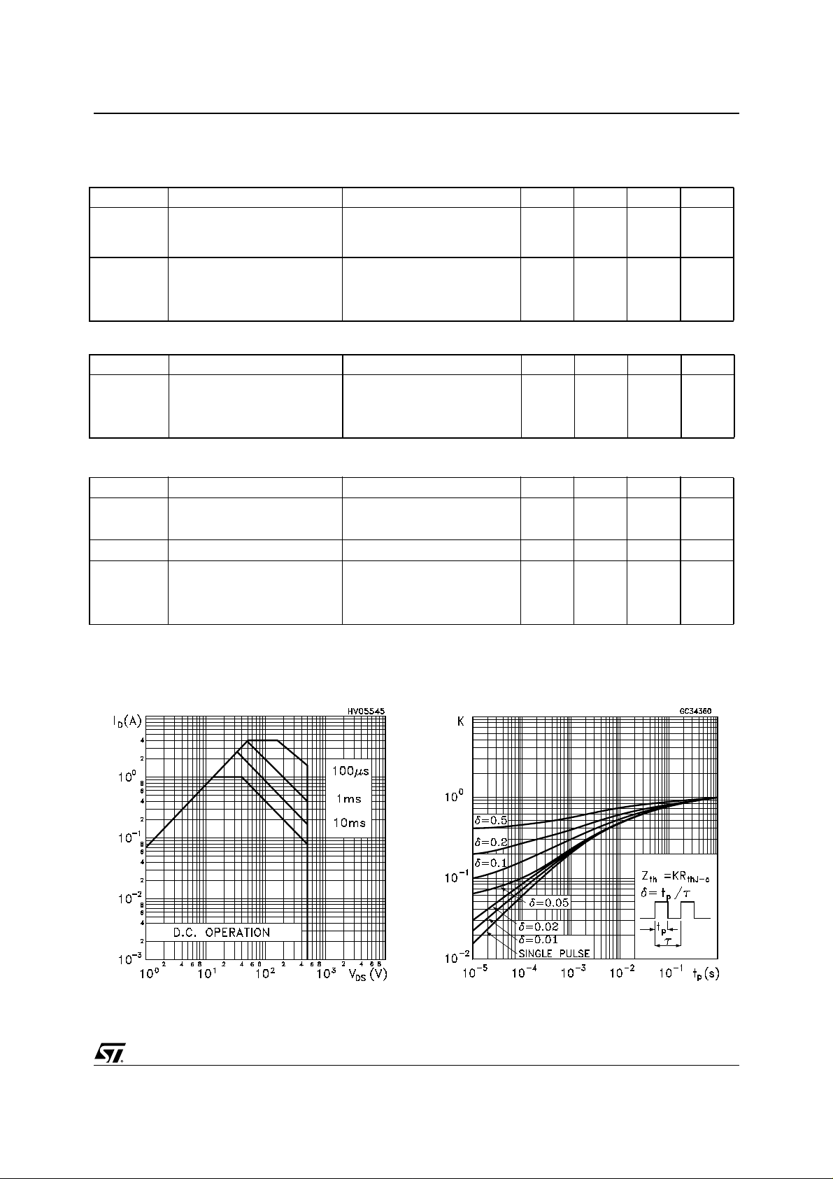
Thermal Impedence Safe Operating Area
3/10
 Loading...