

SGS Thomson Microelectronics STD20N06 Datasheet
STD20N06
N - CHANNEL ENHANCEMENT MODE
”ULTRA HIGH DENSITY” POWER MOS TRANSISTOR
PRELIMINARY DATA
TYPE V
DSS
R
DS(on)
I
D
STD 20N06 60 V < 0.03 Ω 20 A (*)
■ TYPICAL R
■ AVALANCHE RUGGED TECHNOLOGY
■ 100% AVALANCHE TESTED
■ REPETITIVE AVALANCHE DATA AT 100
■ HIGH CURRENT CAPABILITY
o
■ 175
■ HIGH dV/dt RUGGEDNESS
■ THROUGH-HOLE IPAK (TO-251) POWER
C OPERATING TEMPERATURE
DS(on)
= 0.026 Ω
o
C
PACKAGE IN TUBE (SUFFIX ”-1”)
■ SURFACE-MOUNTINGDPAK (TO-252)
POWER PACKAGE IN TAPE & REEL
(SUFFIX ”T4”)
DESCRIPTION
This series of POWER MOSFETS represents the
latest development in low voltage technology.
The ultra high cell density process (UHD) produced with fine geometries on advanced equipment
gives the device extremely low R
DS(on)
as well as
good switching performance and high avalanche
energy capability.
APPLICATIONS
■ HIGH CURRENT, HIGH SPEED SWITCHING
■ POWER MOTOR CONTROL
■ DC-DC & DC-AC CONVERTERS
■ SYNCRONOUS RECTIFICATION
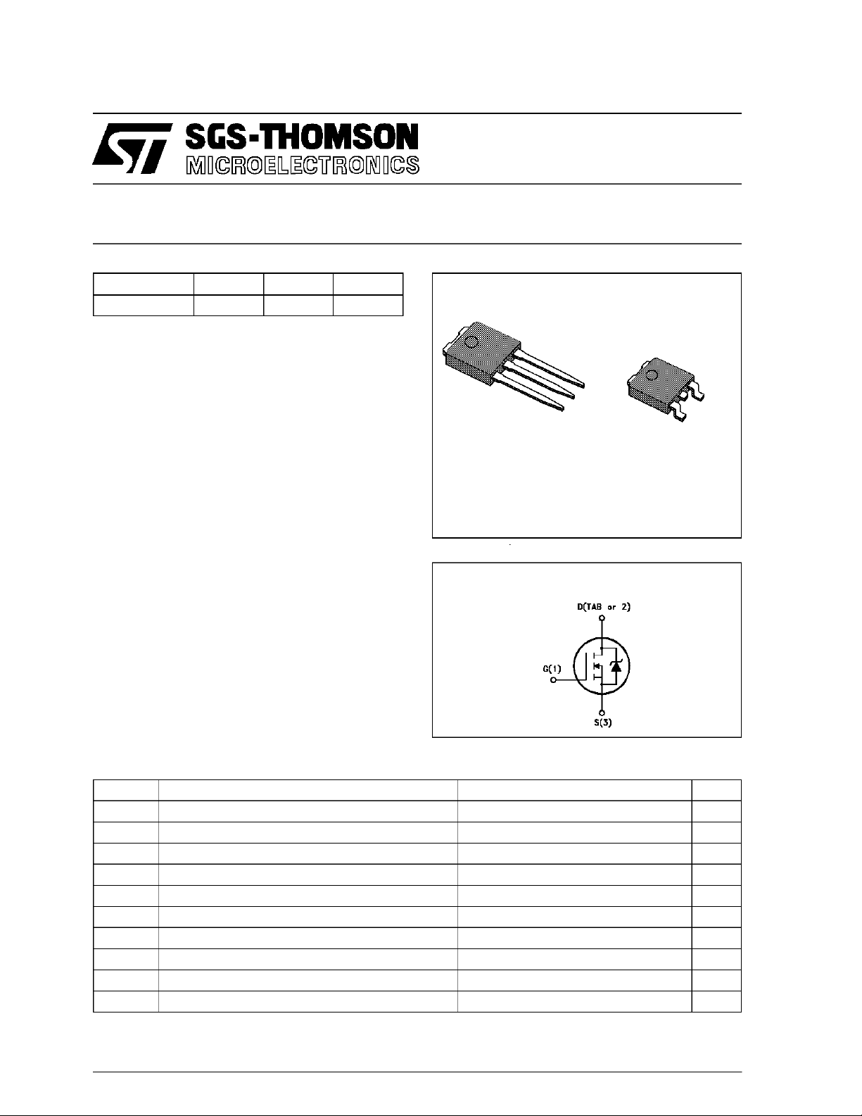
3
2
1
IPAK
TO-251
(Suffix ”-1”)
INTERNAL SCHEMATIC DIAGRAM
1
DPAK
TO-252
(Suffix ”T4”)
3
ABSOLUTE MAXIMUM RATINGS
Symb o l Paramet er Val u e Unit
V
V
V
I
DM
P
T
(*) Currentlimited by the package
(•) Pulse width limited by safeoperating area (*)
March 1995
Drain - s ource Voltage (VGS=0) 60 V
DS
Drain- gate Voltage (RGS=20kΩ)60V
DGR
Gate-source Voltage ± 20 V
GS
Drain Current (continuous) at Tc=25oC20A
I
D
Drain Current (continuous) at Tc=100oC14A
I
D
(•) Drain Current (pulsed) 80 A
Total Di ssipation at Tc=25oC60W
tot
Derat ing Factor 0.4 W/
St or a ge Tem perature -65 to 175
stg
Max. Operating Junction Temperature 175
T
j
o
o
o
C
C
C
1/10
STD20N06
THERMAL DATA
R
thj-case
R
thj-amb
R
thj-amb
T
AVALANCHE CHARACTERISTICS
Symbol Parameter Max Valu e Uni t
I
AR
E
E
I
AR
Thermal Res is tance Junction- c ase Max
Thermal Res istance Junc tion-am bie nt Max
Thermal Res is tance Case-sink Typ
Maximum Lead Tem perature Fo r Soldering Pu r pose
l
Avalanc h e Cu rr ent , Repet itive or Not-R ep et itive
(pulse width limited by Tjmax, δ <1%)
Single Pul se Avalanche Ener gy
AS
(starti ng T
=25oC, ID=IAR, L = 330 µH, VDD=25V)
j
(see waveforms, figure 2)
Repetitive Avalanc he Energ y
AR
(pulse width limited by Tjmax, δ <1%)
Avalanc h e Cu rr ent , Repet itive or Not-R ep et itive
(Tc= 100oC, pulse width limit ed by Tjmax, δ <1%)
2.5
100
1.5
300
20 A
80 mJ
20 mJ
14 A
o
C/W
o
C/W
o
C/W
o
C
ELECTRICAL CHARACTERISTICS (T
=25oC unless otherwise specified)
case
OFF
Symbol Parameter Test Condition s Min. Typ. Max. U nit
V
(BR)DSS
Drain - s ource
ID=250µAVGS=0 60 V
Break d own Volta ge
I
DSS
I
GSS
Zer o Gate Volt age
Drain Current (VGS=0)
Gat e- body Leak age
VDS=MaxRating
VDS= Max Rating x 0 .8 Tc=125oC
250
1000µAµA
VGS= ± 20 V ± 10 0 nA
Current (VDS=0)
ON (∗)
Symbol Parameter Test Condition s Min. Typ. Max. U nit
V
GS(th)
R
DS(on)
I
D(on)
Gate Threshold Voltage VDS=VGSID=250µA234V
St at ic Drain-s our ce O n
Resistance
On State Drain Current VDS>I
VGS=10V ID=10A
VGS=10V ID=10A Tc= 100oC
D(on)xRDS(on)max
0.026 0.03
0.06
20 A
VGS=10V
DYNAMIC
Symbol Parameter Test Condition s Min. Typ. Max. U nit
(∗)Forward
g
fs
Tr ansconductance
C
C
C
Input Capacitance
iss
Out put Capacitance
oss
Reverse Transfer
rss
Capacitance
VDS>I
D(on)xRDS(on)maxID
=10A 11 16 S
VDS=25V f=1MHz VGS= 0 2000
350
80
2800
450
120
Ω
Ω
pF
pF
pF
2/10
STD20N06
ELECTRICAL CHARACTERISTICS (continued)
SWITCHING ON
Symbol Parameter Test Condition s Min. Typ. Max. U nit
t
d(on)
(di/dt)
Q
Q
Q
Turn-on T im e
t
Rise Time
r
Turn-on C urrent S lope VDD=48V ID=20A
on
Total Gate Charge
g
Gat e- Source Charge
gs
Gate-Drain Charge
gd
SWITCHING OFF
Symbol Parameter Test Condition s Min. Typ. Max. U nit
t
r(Voff)
t
Off -voltage R ise Time
t
Fall Time
f
Cross-over Time
c
SOURCE DRAIN DIODE
VDD=30V ID=10A
RG=50 Ω VGS=10V
45
28065380
(see test circuit, figure 3)
240 A/µs
RG=50 Ω VGS=10V
(see test circuit, figure 5)
VDD=40V ID=20A VGS=10V 60
10
20
VDD=48V ID=20A
RG=50 Ω VGS=10V
(see test circuit, figure 5)
55
125
200
80 nC
75
170
270
ns
ns
nC
nC
ns
ns
ns
Symbol Parameter Test Condition s Min. Typ. Max. U nit
I
I
SDM
SD
Source-drain Current
(•)
Source-drain Current
20
80
(pulsed)
V
(∗) Forward On Volt age ISD=20A VGS=0 1.5 V
SD
t
Reverse Recovery
rr
Time
Q
Reverse Recovery
rr
ISD= 20 A di/dt = 100 A/µs
VDD=30V Tj=150oC
(see test circuit, figure 5)
80
0.3
Charge
I
RRM
Reverse Recovery
7
Current
(∗) Pulsed:Pulse duration = 300 µs, dutycycle 1.5 %
(•) Pulse widthlimited by safeoperating area
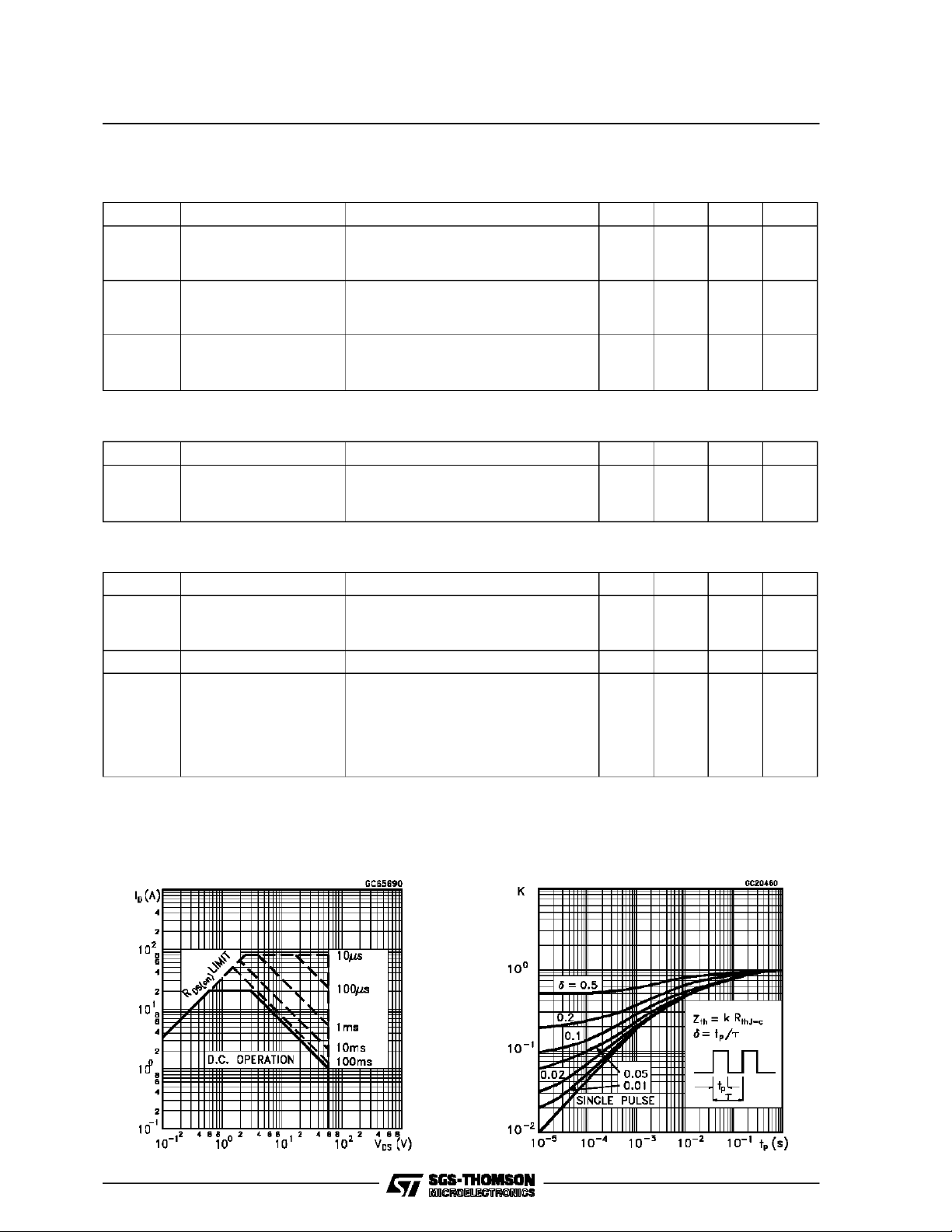
Safe Operating Area Thermal Impedance
A
A
ns
µC
A
3/10
 Loading...