

STD17N05
STD17N06
N - CHANNEL ENHANCEMENT MODE
POWER MOS TRANSISTOR
TYPE V
DSS
R
DS(on)
I
D
STD 17N05 50 V < 0.085 Ω 17 A
STD 17N06 60 V < 0.085 Ω 17 A
■ TYPICAL R
■ AVALANCHE RUGGED TECHNOLOGY
■ 100% AVALANCHE TESTED
■ REPETITIVE AVALANCHE DATA AT 100
■ LOW GATE CHARGE
■ HIGH CURRENT CAPABILITY
o
■ 175
■ APPLICATION ORIENTED
C OPERATING TEMPERATURE
DS(on)
= 0.06 Ω
o
C
CHARACTERIZATION
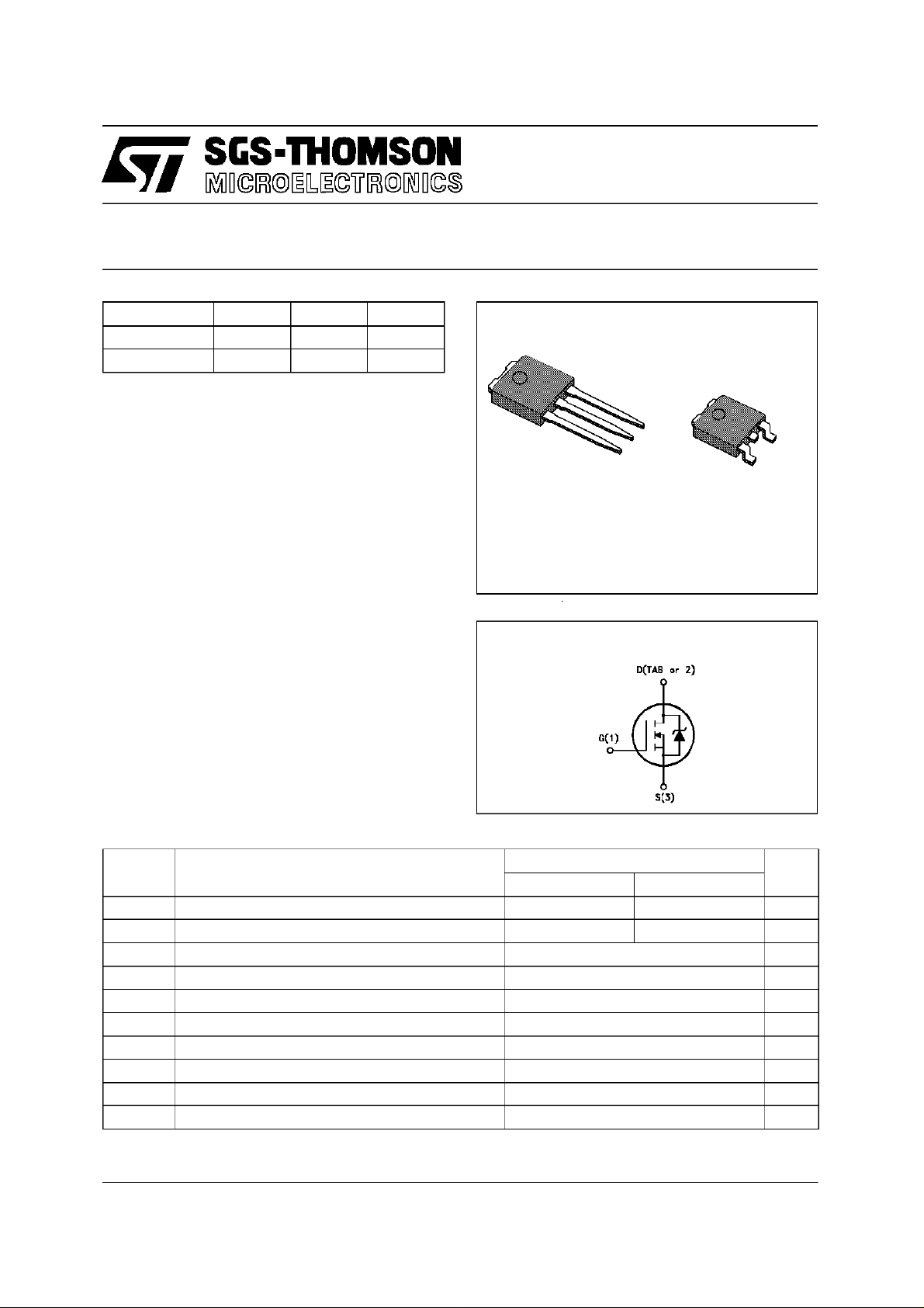
■ THROUGH-HOLE IPAK (TO-251) POWER
PACKAGE IN TUBE (SUFFIX ”-1”)
■ SURFACE-MOUNTINGDPAK (TO-252)
POWER PACKAGE IN TAPE & REEL
(SUFFIX ”T4”)
APPLICATIONS
■ HIGH CURRENT, HIGH SPEED SWITCHING
■ SOLENOID AND RELAY DRIVERS
■ REGULATORS
■ DC-DC & DC-AC CONVERTERS
■ MOTOR CONTROL, AUDIO AMPLIFIERS
■ AUTOMOTIVE ENVIRONMENT (INJECTION,
ABS, AIR-BAG, LAMPDRIVERS, Etc.)
3
2
1
IPAK
TO-251
(Suffix ”-1”)
INTERNAL SCHEMATIC DIAGRAM
1
DPAK
TO-252
(Suffix ”T4”)
3
ABSOLUTE MAXIMUM RATINGS
Symb o l Paramet er Val u e Unit
ST D17N05 STD17N06
V
V
V
I
DM
P
T
(•) Pulsewidth limited bysafe operating area
December 1996
Drain - s ource Voltage (VGS=0) 50 60 V
DS
Drain- gate Voltage (RGS=20kΩ)5060V
DGR
Gate-source Voltage ± 20 V
GS
Drain Current (continuous) at Tc=25oC17A
I
D
Drain Current (continuous) at Tc=100oC12A
I
D
(•) Drain Current (pulsed) 68 A
Total Di ssipation at Tc=25oC55W
tot
Derating F actor 0.37 W/
St or a ge Tem perature -65 to 175
stg
Max. Operating Junction Temperature 175
T
j
o
o
o
C
C
C
1/10
STD17N05/STD17N06
THERMAL DATA
R
thj-case
R
thj-amb
R
thc-sink
T
AVALANCHE CHARACTERISTICS
Symbol Parameter Max Value Uni t
I
AR
E
E
I
AR
Thermal Resistance Junction - cas e Max
Thermal Resistance Junction- ambient Max
Thermal Resistance Case-sink Typ
Maximum Lead T emperature For Soldering Purpose
l
Avalanc h e Cu rr ent , Repet itive or Not-R ep et itive
(pulse width limited by Tjmax, δ <1%)
Single Pul se Avalanche Ener gy
AS
(starti ng Tj=25oC, ID=IAR,VDD=25V)
Repetitive Avalanc he Energ y
AR
(pulse width limited by Tjmax, δ <1%)
Avalanc h e Cu rr ent , Repet itive or Not-R ep et itive
(Tc= 100oC, pulse width limited by Tjmax, δ <1%)
2.73
100
1.5
275
17 A
60 mJ
15 mJ
12 A
o
C/W
o
C/W
o
C/W
o
C
ELECTRICAL CHARACTERISTICS (T
=25oC unless otherwise specified)
case
OFF
Symbol Parameter Test Co ndition s Min. Typ. Max. Unit
V
(BR)DSS
I
DSS
I
GSS
Drain - s ource
Break d own Volta ge
Zer o Gate Volt age
Drain Current (VGS=0)
Gat e- body Leak age
ID=250µAVGS=0
for STD17N05
for STD17N06
VDS=MaxRating
VDS= Max Rating x 0 .8 Tc=125oC
50
60
1
10
VGS= ± 20 V ± 100 nA
Current (VDS=0)
ON (∗)
Symbol Parameter Test Co ndition s Min. Typ. Max. Unit
V
GS(th)
R
DS(on)
Gate Threshold Voltage VDS=VGSID=250µA22.94V
St at ic Drain-s our ce O n
VGS=10V ID= 8.5 A 0.06 0.085 Ω
Resistance
I
D(on)
On State Drain Current VDS>I
D(on)xRDS(on)max
17 A
VGS=10V
DYNAMIC
Symbol Parameter Test Co ndition s Min. Typ. Max. Unit
(∗)Forward
g
fs
Tr ansconductance
C
C
C
Input Capacitance
iss
Out put Capacitance
oss
Reverse Transfer
rss
Capacitance
VDS>I
D(on)xRDS(on)maxID
=8.5A 5 8 S
VDS=25V f=1MHz VGS=0 600
250
80
800
350
120
V
V
µA
µA
pF
pF
pF
2/10
STD17N05/STD17N06
ELECTRICAL CHARACTERISTICS (continued)
SWITCHING ON
Symbol Parameter Test Co ndition s Min. Typ. Max. Unit
t
d(on)
(di/dt)
Q
Q
Q
Turn-on T im e
t
Rise Time
r
Turn-on C urrent S lope VDD=40V ID=17A
on
Total Gate Charge
g
Gat e- Source Charge
gs
Gate-Drain Charge
gd
SWITCHING OFF
Symbol Parameter Test Co ndition s Min. Typ. Max. Unit
t
r(Voff)
t
Off -voltage R ise Time
t
Fall Time
f
Cross-over Time
c
SOURCE DRAIN DIODE
VDD=30V ID=8.5A
RG=50 Ω VGS=10V
20
12030170
(see test circ uit figure)
250 A/µs
RG=50 Ω VGS=10V
(see test circ uit figure)
VDD=40V ID=17A VGS=10V 22
8
8
VDD=40V ID=17A
RGS=50 Ω VGS=10V
(see test circ uit figure)
60
60
120
30 nC
90
90
180
ns
ns
nC
nC
ns
ns
ns
Symbol Parameter Test Co ndition s Min. Typ. Max. Unit
I
I
SDM
SD
Source-drain Current
(•)
Source-drain Current
17
68
(pulsed)
V
(∗) Forward On Volt age ISD=17A VGS=0 1.5 V
SD
t
Reverse Recovery
rr
Time
Q
Reverse Recovery
rr
ISD= 17 A di/dt = 100 A/µs
VDD=30V Tj=150oC
65
0.13
Charge
I
RRM
Reverse Recovery
4
Current
(∗) Pulsed:Pulse duration = 300 µs, dutycycle 1.5 %
(•) Pulse widthlimited by safeoperating area
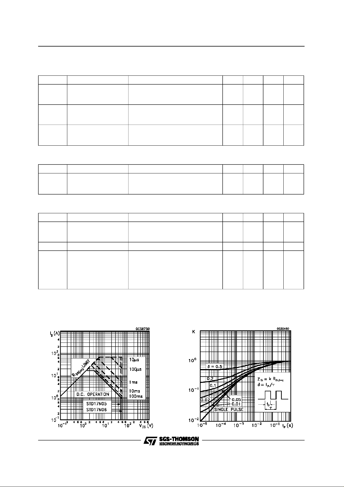
Safe Operating Area Thermal Impedance
A
A
ns
µC
A
3/10

STD17N05/STD17N06
Derating Curve
Transfer Characteristics
Output Characteristics
Transconductance
Static Drain-source On Resistance
4/10
Gate Charge vs Gate-source Voltage

STD17N05/STD17N06
Capacitance Variations Normalized Gate Threshold Voltage vs
Temperature
Normalized On Resistance vs Temperature Turn-on Current Slope
Cross-over TimeTurn-off Drain-source Voltage Slope
5/10

STD17N05/STD17N06
Switching SafeOperating Area Accidental Overload Area
Source-drain Diode Forward Characteristics
Fig. 1: Unclamped Inductive Load Test Circuits Fig. 2: Unclamped Inductive Waveforms
6/10

STD17N05/STD17N06
Fig. 3: Switching Times Test Circuits For
Resistive Load
Fig. 5: Test Circuit For Inductive Load Switching
And Diode Recovery Times
Fig. 4: Gate Charge Test Circuit
7/10

STD17N05/STD17N06
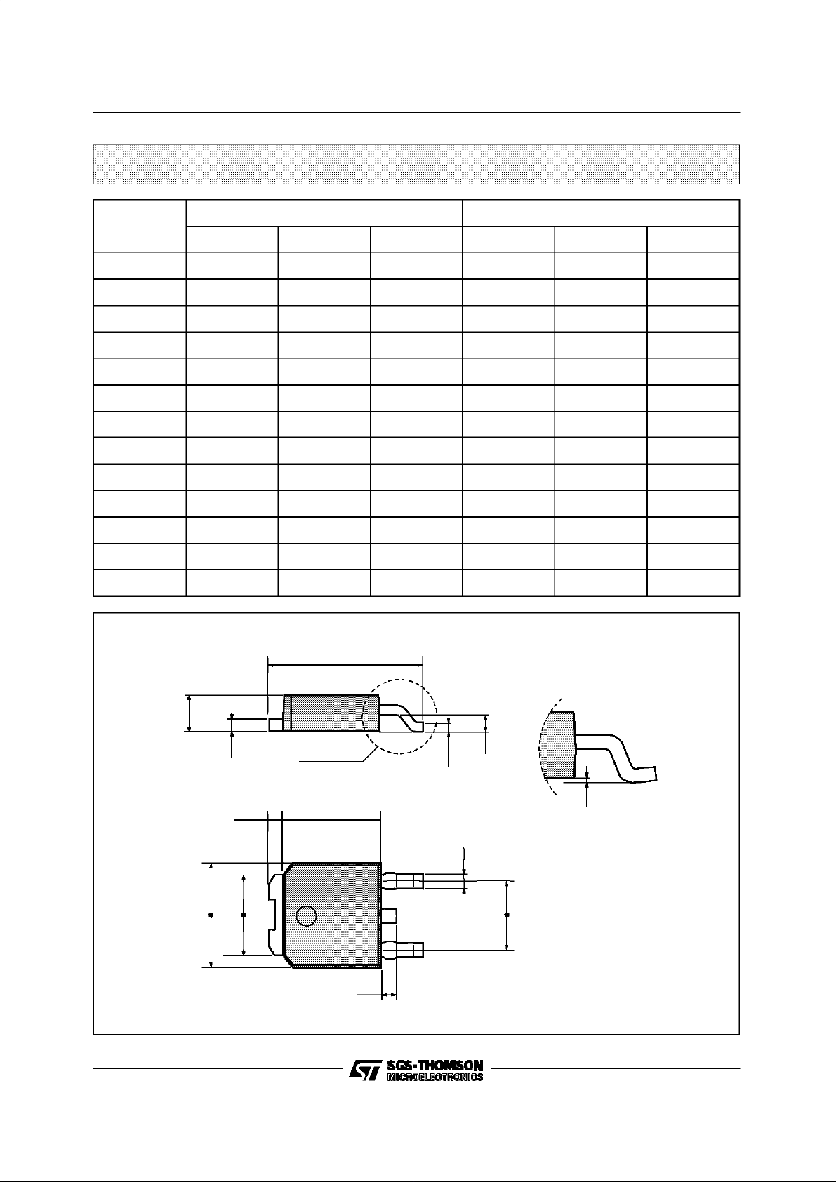
TO-251 (IPAK) MECHANICAL DATA
DIM.
mm inch
MIN. TYP. MAX. MIN. TYP. MAX.
A 2.2 2.4 0.086 0.094
A1 0.9 1.1 0.035 0.043
A3 0.7 1.3 0.027 0.051
B 0.64 0.9 0.025 0.031
B2 5.2 5.4 0.204 0.212
B3 0.85 0.033
B5 0.3 0.012
B6 0.95 0.037
C 0.45 0.6 0.017 0.023
C2 0.48 0.6 0.019 0.023
D 6 6.2 0.236 0.244
E 6.4 6.6 0.252 0.260
G 4.4 4.6 0.173 0.181
H 15.9 16.3 0.626 0.641
L 9 9.4 0.354 0.370
L1 0.8 1.2 0.031 0.047
L2 0.8 1 0.031 0.039
8/10
A
E
==
C2
L2
B2
==
H
C
A3
A1
B6
L
B
B5
G
==
D
B3
2
13
L1
0068771-E
TO-252 (DPAK) MECHANICAL DATA
STD17N05/STD17N06
DIM.
mm inch
MIN. TYP. MAX. MIN. TYP. MAX.
A 2.2 2.4 0.086 0.094
A1 0.9 1.1 0.035 0.043
A2 0.03 0.23 0.001 0.009
B 0.64 0.9 0.025 0.035
B2 5.2 5.4 0.204 0.212
C 0.45 0.6 0.017 0.023
C2 0.48 0.6 0.019 0.023
D 6 6.2 0.236 0.244
E 6.4 6.6 0.252 0.260
G 4.4 4.6 0.173 0.181
H 9.35 10.1 0.368 0.397
L2 0.8 0.031
L4 0.6 1 0.023 0.039
H
A
E
==
C2
L2
B2
==
DETAIL”A”
D
2
13
L4
A1
C
A2
DETAIL”A”
B
G
==
0068772-B
9/10

STD17N05/STD17N06
Information furnished is believed to be accurate and reliable. However, SGS-THOMSON Microelectronics assumes no responsability for the
consequences of useof such informationnor for any infringement of patents or other rightsof third parties which mayresults fromits use. No
licenseis granted by implication orotherwise under any patentor patent rights of SGS-THOMSONMicroelectronics. Specificationsmentioned
in thispublication are subject to change withoutnotice. Thispublication supersedes andreplacesall informationpreviously supplied.
SGS-THOMSONMicroelectronics products are not authorizedfor use ascriticalcomponents in lifesupportdevicesor systems withoutexpress
writtenapproval ofSGS-THOMSONMicroelectonics.
1996 SGS-THOMSON Microelectronics -Printed in Italy- AllRightsReserved
Australia- Brazil -Canada -China - France- Germany - HongKong- Italy - Japan- Korea- Malaysia - Malta- Morocco - The Netherlands -
Singapore - Spain - Sweden - Switzerland-Taiwan - Thailand- UnitedKingdom - U.S.A
SGS-THOMSONMicroelectronics GROUPOF COMPANIES
.
10/10
 Loading...