

SGS Thomson Microelectronics STD10NF06L Datasheet
STD10NF06L
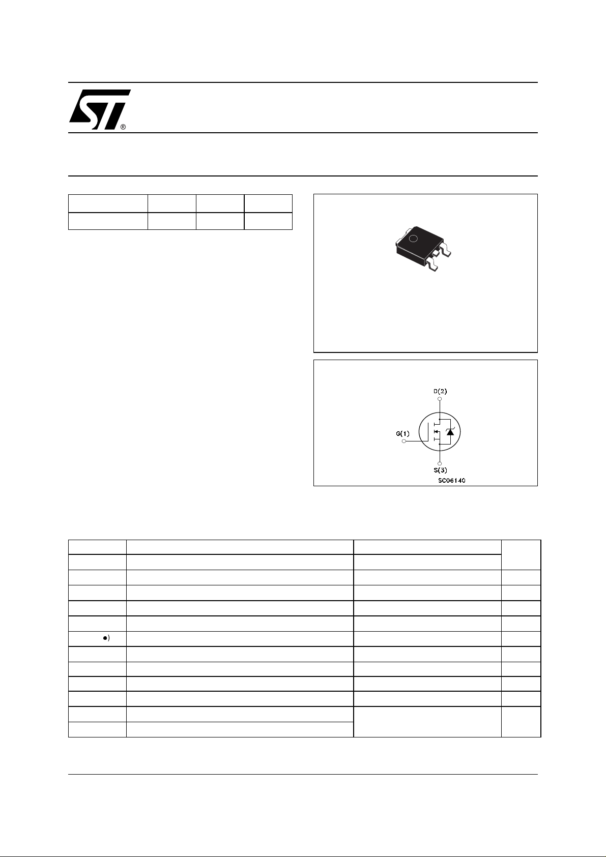
N-CHANNEL 60V - 0.1Ω - 10A DPAK
STripFET™ POWER MOSFET
PRELIMINARY DATA
TYPE V
STD10NF06L 60V <0.12Ω 10A
■ TYPICAL R
■ SURFACE-MOUNTING DPAK (TO-252) POWER
DS
DSS
(on) = 0.1Ω
R
DS(on)
I
D
PACKAGE IN TAPE & REEL (SUFFIX “T4”)
DESCRIPTION
This MOSFET series realized with STMicroelectronics
unique STripFET
™ process has specifically been de-
signed to minimize input capacitance and gate charge.
It is therefore suitable as primary swi tch in advanced
high-efficiency, high-frequency isolated DC-DC converters for Telecom and Computer applications. It is
also intended for any applications with low gate drive
requirements.
APPLICATIONS
■ DC-DC & DC-AC CONVERTERS
■ DC MOTOR CONTROL
3
1
DPAK
INTERNAL SCHEMATIC DIAGRAM
ABSOLUTE MAXIMUM RATINGS
Symbol Parameter Value Unit
V
DS
V
DGR
V
GS
I
D
I
D
I
DM
P
TOT
dv/dt (1) Peak Diode Recovery voltage slope 30 V/ns
E
AS
T
stg
T
j
(●) Pulse width limited by safe operating area
November 2001
This is preliminary information on a new product now in development or undergoing evaluation. Details are subject to change without notice.
Drain-source Voltage (VGS = 0)
Drain-gate Voltage (RGS = 20 kΩ)
Gate- source Voltage ± 15 V
Drain Current (continuos) at TC = 25°C
Drain Current (continuos) at TC = 100°C
(l)
Drain Current (pulsed) 40 A
Total Dissipation at TC = 25°C
Derating Factor 0.2 W/°C
(2)
Single Pulse Avalanche Energy 50 mJ
Storage Temperature
Max. Operating Junction Temperature
(1) ISD ≤10A, di/dt ≤400A/µs, VDD =48V, Tj ≤ T
(2) Starting Tj = 25°C, Id = 7A, VDD=20 V
60 V
60 V
10 A
7A
30 W
– 55 to 175 °C
JMAX.
1/7
STD10NF06L
THERMA L D ATA
Rthj-case Thermal Resistance Junction-case Max 5 °C/W
Rthj-amb Thermal Resistance Junction-ambient Max 100 °C/W
T
l
ELECTRICAL CHARACTERISTICS (TCASE = 25 °C UNLESS OTHERWISE SPECIFIED)
OFF
Symbol Parameter Test Conditions Min. Typ. Max. Unit
V
(BR)DSS
I
DSS
I
GSS
ON
(1)
Symbol Parameter Test Conditions Min. Typ. Max. Unit
V
GS(th)
R
DS(on)
Maximum Lead Temperature For Soldering Purpose 275 °C
Drain-source
ID = 250 µA, VGS = 0 60 V
Breakdown Voltage
Zero Gate Voltage
Drain Current (V
GS
= 0)
Gate-body Leakage
Current (V
DS
= 0)
Gate Threshold Voltage
Static Drain-source On
Resistance
V
= Max Rating
DS
V
= Max Rating, TC = 125 °C
DS
V
= ± 15V ±100 nA
GS
V
= VGS, ID = 250µA
DS
VGS = 10V, ID = 5 A
VGS = 5 V, ID = 5 A
1V
0.1 0.12 Ω
0.12 0.14 Ω
1µA
10 µA
DYNAMIC
Symbol Parameter Test Conditions Min. Typ. Max. Unit
(1) Forward Transconductance VDS =15 V , ID=10A
g
fs
C
iss
C
oss
C
rss
Input Capacitance
Output Capacitance 54 pF
Reverse Transfer
Capacitance
V
= 25V, f = 1 MHz, VGS = 0
DS
6S
346 pF
22 pF
2/7
STD10NF06L
ELECTRICAL CHARACTERISTICS (CONTINUED)
SWITCHING ON
Symbol Parameter Test Conditions Min. Typ. Max. Unit
V
t
d(on)
Q
Q
Q
t
r
g
gs
gd
Turn-on Delay Time
Rise Time 50 ns
Total Gate Charge
Gate-Source Charge
Gate-Drain Charge
SWITCHING OFF
Symbol Parameter Test Conditions Min. Typ. Max. Unit
t
d(off)
t
f
Turn-off-Delay Time
Fall Time
SOURCE DRAIN DIODE
Symbol Parameter Test Conditions Min. Typ. Max. Unit
I
SD
I
SDM
VSD (1)
t
rr
Q
rr
I
RRM
Note: 1. Pulsed: Pu l se duration = 300 µs, duty c yc l e 1.5 %.
2. Pulse width li mited by safe operating area.
Source-drain Current 10 A
(2)
Source-drain Current (pulsed) 40 A
Forward On Voltage
Reverse Recovery Time
Reverse Recovery Charge
Reverse Recovery Current
= 30V, ID = 5A
DD
RG= 4.7Ω VGS = 4.5V
(see test circuit, Figure 3)
= 48V, ID = 10A,
V
DD
VGS = 5V
= 30V, ID = 5A,
V
DD
RG=4.7Ω, V
GS
= 4.5V
(see test circuit, Figure 5)
ISD = 10A, VGS = 0
= 10A, di/dt = 100A/µs,
I
SD
VDD = 20V, Tj = 150°C
(see test circuit, Figure 5)
10 ns
6
8
3
2.5
20
10
1.3 V
30
50
3
nC
nC
nC
ns
ns
ns
nC
A
3/7
 Loading...