

SGS Thomson Microelectronics STC5NF20V Datasheet

STC5NF20V
N-CHANNEL 20V - 0.030 Ω - 5A TSSOP8
2.7V-DRIVE STripFET™ II POWER MOSFET
TYPE
V
DSS
STC5NF20V 20 V
■ TYPICAL R
■ TYPICAL R
■ ULTRA LOW THRESHOLD
(on) = 0.030 Ω @ 4.5 V
DS
(on) = 0.037 Ω @ 2.7 V
DS
R
DS(on)
< 0.040 Ω ( @ 4.5 V )
< 0.045 Ω ( @ 2.7 V )
I
D
5 A
GATE DRIVE (2.7 V)
■ STANDARD OUTLI NE FO R EASY
AUTOMATED SURFACE MOUNT ASSEMBLY
DESCRIPTION
This Power MOSFET is the latest dev elo pment of
STMicroelectronis unique "Single Feature Size™"
strip-based process. The resulting transistor
shows extremely high packing density for low onresistance, rugged avalanche characteristics and
less critical alignment steps therefore a remarkable manufacturing reproducibility.
APPLICATIONS
■ DC MOTOR DRIVE
■ DC-DC CONVERTERS
■ BATTERY MANAGEMENT IN NOMADIC
EQUIPMENT
■ POWER MANAGEMENT IN
PORTABLE/DESKTOP PCs
TSSOP8
INTERNAL SCHEMATIC DIAGRAM
ABSOLUTE MAXIMUM RATINGS
Symbol Parameter Value Unit
V
DS
V
DGR
V
GS
I
D
I
D
(
I
DM
P
tot
(
Pulse widt h l i m i ted by safe operating area.
•)
.
Drain-source Voltage (VGS = 0)
Drain-gate Voltage (RGS = 20 kΩ)
20 V
20 V
Gate- source Voltage ± 12 V
Drain Current (continuous) at TC = 25°C
Drain Current (continuous) at TC = 100°C
•)
Drain Current (pulsed) 20 A
Total Dissipation at TC = 25°C
5A
3A
1.5 W
1/8February 2003

STC5NF20V
THERMA L D ATA
Rthj-pcb
Rthj-pcb
T
T
stg
(*) When Mounted on FR-4 board with 1 inch
(**) When Mounted on minimum recommended footprint
Thermal Resistance Junction-PCB (**)
Thermal Resistance Junction-PCB (*)
Operating Junction Temperature
j
Storage temperature
2
pad, 2 oz of Cu a nd t [ 10 sec
Max
Max
100
83.5
-55 to 150
-55 to 150
°C/W
°C/W
°C
°C
ELECTRICAL CHARACTERISTICS (T
= 25 °C unless otherwise specified)
case
OFF
Symbol Parameter Test Conditions Min. Typ. Max. Unit
I
V
(BR)DSS
Drain-source
= 250 µA, VGS = 0
D
20
Breakdown Voltage
V
= Max Rating
DS
V
= Max Rating TC = 125°C
DS
= ± 12V
V
GS
1
10
±100 nA
ON
(*)
I
DSS
I
GSS
Zero Gate Voltage
Drain Current (V
GS
Gate-body Leakage
Current (V
DS
= 0)
= 0)
Symbol Parameter Test Conditions Min. Typ. Max. Unit
V
V
GS(th)
R
DS(on)
Gate Threshold Voltage
Static Drain-source On
Resistance
= VGS ID = 250 µA
DS
= 4.5 V ID = 2.5 A
V
GS
V
= 2.7 V ID = 2.5 A
GS
0.6 V
0.030
0.037
0.040
0.045
DYNAMIC
Symbol Parameter Test Conditions Min. Typ. Max. Unit
(*)
g
fs
C
iss
C
oss
C
rss
Forward Transconductance
Input Capacitance
Output Capacitance
Reverse Transfer
Capacitance
V
=15 V ID= 2.5 A
DS
= 15V f = 1 MHz, VGS = 0
V
DS
9.5 S
460
200
50
V
µA
µA
Ω
Ω
pF
pF
pF
2/8
STC5NF20V
ELECTRICAL CHARACTERISTICS (continued)
SWITCHING ON
Symbol Parameter Test Conditions Min. Typ. Max. Unit
= 10 V ID = 2.5 A
t
d(on)
Turn-on Delay Time
t
r
Rise Time
V
DD
R
= 4.7 Ω VGS = 4.5 V
G
(Resistive Load, Figure 1)
Q
g
Q
gs
Q
gd
Total Gate Charge
Gate-Source Charge
Gate-Drain Charge
= 16V ID= 5A VGS=4.5V
V
DD
(see test circuit, Figure 2)
SWITCHING OFF
Symbol Parameter Test Conditions Min. Typ. Max. Unit
= 10 V ID = 2.5 A
t
d(off)
Turn-off Delay Time
t
f
Fall Time
V
DD
R
= 4.7Ω, V
G
GS
= 4.5 V
(Resistive Load, Figure 1)
7
33
8.5
1.8
2.4
27
10
11.5 nC
ns
ns
nC
nC
ns
ns
t
d(Voff)
t
t
c
Off-voltage Rise Time
f
Fall Time
Cross-over Time
= 16 V ID = 5 A
V
clamp
R
= 4.7Ω, V
G
GS
(Inductive Load, Figure 3)
= 4.5 V
26
11
21
SOURCE DRAIN DIODE
Symbol Parameter Test Conditions Min. Typ. Max. Unit
I
SD
I
SDM
V
SD
t
rr
Q
rr
I
RRM
(*)
Pulsed: P ul se duration = 300 µs, duty cycle 1.5 %.
(
•)Pulse width limited by s afe operating area.
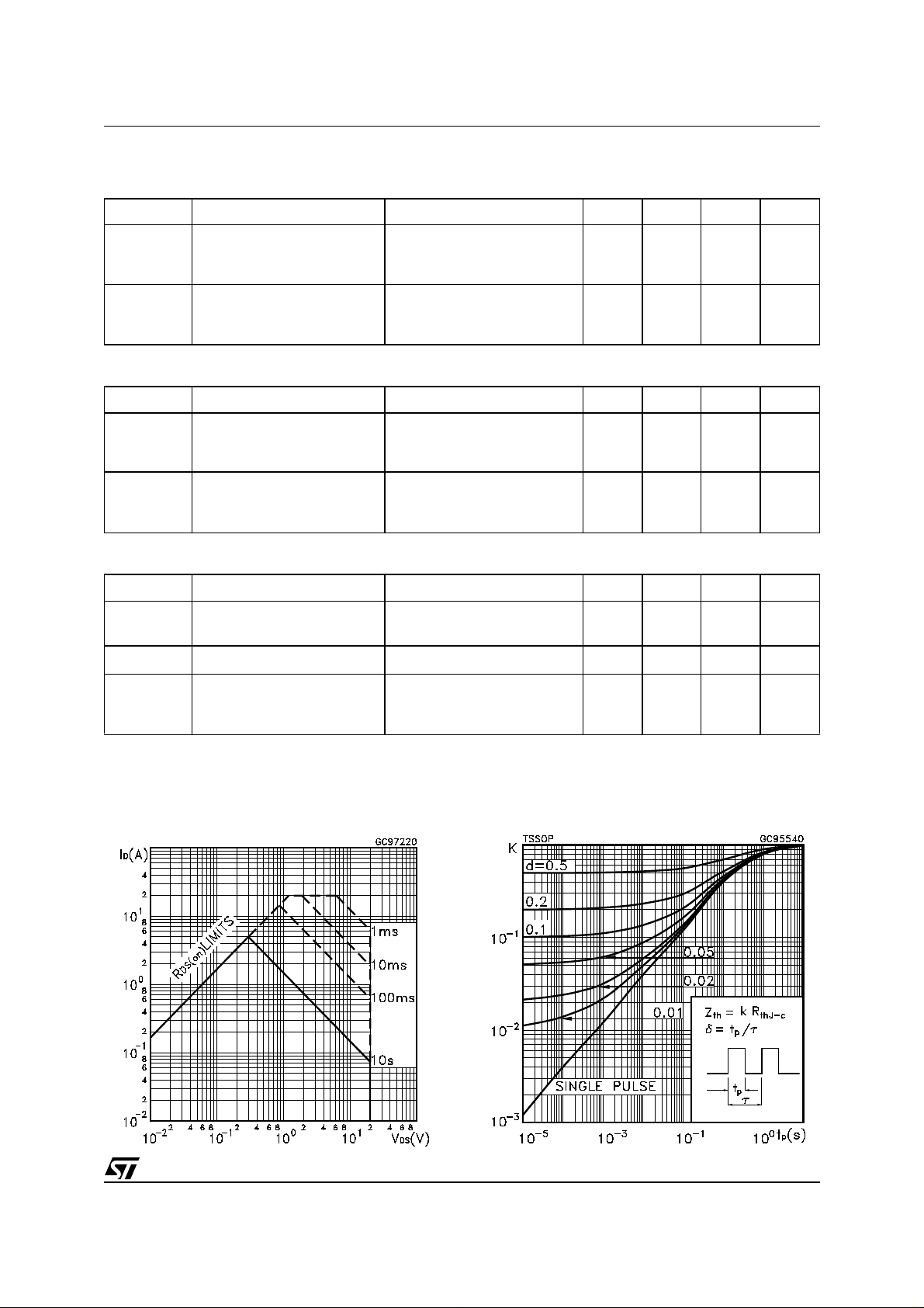
Safe Operating Area
Source-drain Current
(•)
Source-drain Current (pulsed)
(*)
Forward On Voltage
Reverse Recovery Time
Reverse Recovery Charge
Reverse Recovery Current
I
= 5 A VGS = 0
SD
= 5 A di/dt = 100A/µs
I
SD
V
= 10 V Tj = 150°C
DD
(see test circuit, Figure 3)
Thermal Impedance
5
20
1.2 V
26
13
1
ns
ns
ns
A
A
ns
nC
A
3/8
 Loading...