

SGS Thomson Microelectronics STW9NK70Z, STP9NK70ZFP, STP9NK70Z, STB9NK70Z, STB9NK70Z-1 Datasheet
STP9NK70Z - STP9NK70ZFP
STB9NK70Z - STB9NK70Z-1 - STW9NK70Z
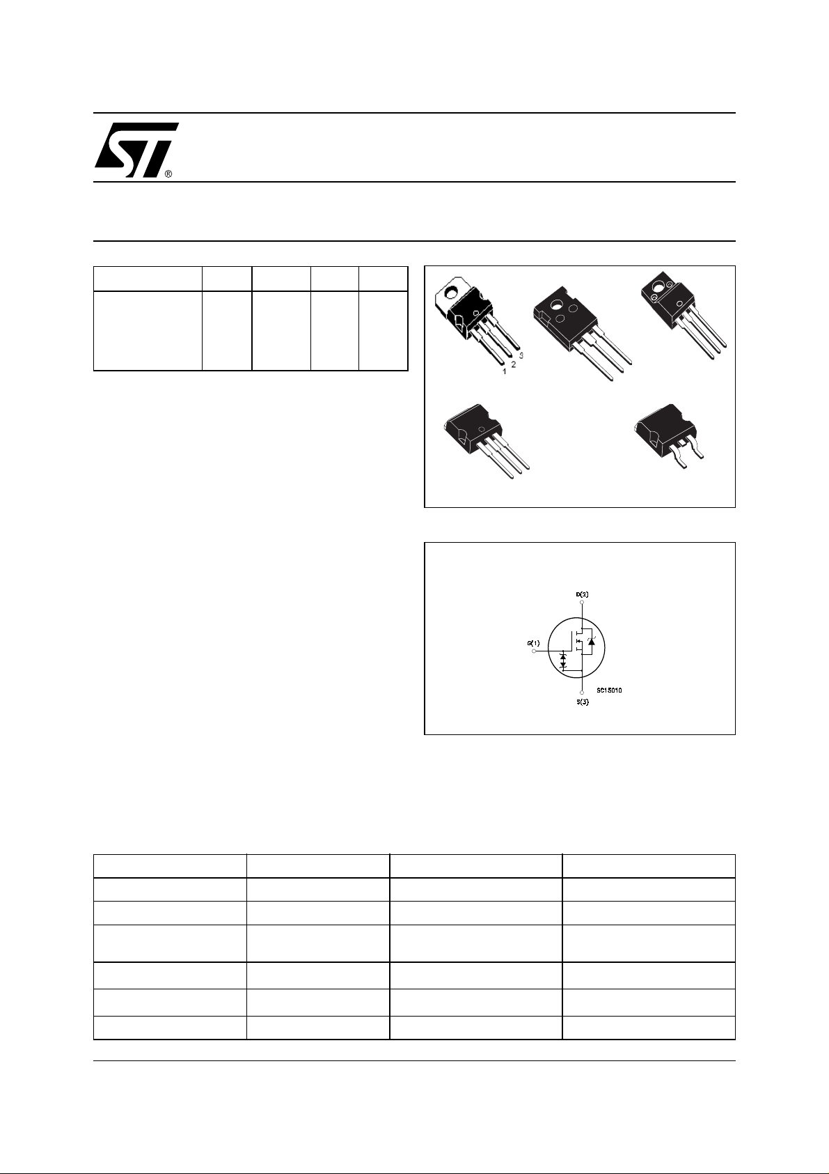
N-CHANNEL 7 00V - 1Ω - 7.5A TO-2 20/FP/D2PAK/I2PAK/TO-247
Zener-Protected SuperMESH™Power MOSFET
TYPE V
STP9NK70Z
STP9NK70ZFP
STB9NK70Z
STB9NK70Z-1
STW9NK70Z
■ TYPICAL R
■ EXTREMELY HIGH dv /d t C APABILITY
■ IMPROVED ESD CAPABILITY
■ 100% AVALANCHE RATED
■ GATE CHARGE MINIMIZED
■ VERY LOW INTRINSIC CAPAC ITANCES
■ VERY GOOD MANUFACTURING
700 V
700 V
700 V
700 V
700 V
(on) = 1.0 Ω
DS
DSS
R
DS(on)
< 1.2 Ω
< 1.2 Ω
< 1.2 Ω
< 1.2 Ω
< 1.2 Ω
I
D
7.5 A
7.5 A
7.5 A
7.5 A
7.5 A
Pw
115 W
35 W
115 W
115 W
156 W
REPEATIBILITY
DESCRIPTION
The SuperMESH™ series is obtained through an
extreme optimization of ST ’s well established stripbased PowerMESH™ layout. In addition to pushing
on-resistance significantly down, special care is taken to ensure a very good dv/dt capability for the
most demanding applications. Such s eries com plements ST full range of high voltage MOSFE Ts including revolutionary MDmesh™ products.
3
2
TO-220 TO-220FP
1
TO-247
3
I2PAK
3
2
1
D
2
PAK
1
INTERNAL SCHEMATIC DIAGRAM
3
2
1
APPLICATIONS
■ HIGH CURRENT, HIGH SPEED SWITCHING
■ IDEAL FOR OFF-LINE POWER SUPP L I ES,
ADAPTORS AND PFC
ORDERING INFORMATION
SALES TYPE MARKING PACKAGE PACKAGING
STP9NK70Z P9NK70Z TO-220 TUBE
STP9NK70ZFP P9NK70ZFP TO-220FP TUBE
STB9NK70Z B9NK70Z
STB9NK70ZT4 B9NK70Z
STB9NK70Z-1 B9NK70Z-1
STW9NK60Z W9NK70Z TO-247 TUBE
2
PAK
D
2
PAK
D
2
I
PAK
(ONLY UNDER REQUEST)
TUBE
TAPE & REEL
TUBE
1/14April 2002
STP9NK70Z / STP9NK70ZFP / STB9NK70Z / STB9NK70Z-1 / STW9NK70Z
ABSOLUTE MAXIMUM RATINGS
Symbol Parameter Value Unit
TO-220 /
2
PAK / I2PAK
D
V
I
DM
P
V
DGR
V
I
I
TOT
DS
GS
D
D
Drain-source Voltage (VGS = 0)
Drain-gate Voltage (RGS = 20 kΩ)
Gate- source Voltage ± 30 V
Drain Current (continuous) at TC = 25°C
Drain Current (continuous) at TC = 100°C
(l)
Drain Current (pulsed) 30 30 (*) 30 A
Total Dissipation at TC = 25°C
7.5 7.5 (*) 7.5 A
4.7 4.7 (*) 4.7 A
115 35 156 W
Derating Factor 0.92 0.28 1.25 W/°C
V
ESD(G-S)
Gate source ESD(HBM-C=100pF, R=1.5KΩ) 4000 V
dv/dt (1) Peak Diode Recovery voltage slope 4.5 V/ns
V
ISO
T
j
T
stg
(l) Pulse wi dth limited by saf e operating area
(1) I
≤7.5A, di/dt ≤200 µA, VDD ≤ V
SD
(*) Limited only by maximum temperature allowed
Insulation Withstand Voltage (DC) - 2500 V
Operating Junction Temperature
Storage Temperature
, Tj ≤ T
(BR)DSS
JMAX.
TO-220FP TO-247
700 V
700 V
-55 to 150
-55 to 150
°C
°C
THERMA L D ATA
TO-220
2
PAK
I
Rthj-case Thermal Resistance Junction-case Max 1.09 3.6 0.8 °C/W
Rthj-pcb
Thermal Resistance Junction-pcb Max
(When mounted on minimum Footprint)
Rthj-amb Thermal Resistance Junction-ambient Max 62.5 30 °C/W
T
l
Maximum Lead Temperature For Soldering Purpose
2
D
TO-220FP TO-247
PAK
30 °C/W
300 °C
AVALANCHE CHARACTERISTICS
Symbol Parameter Max Value Unit
I
AR
E
AS
Avalanche Current, Repetitive or Not-Repetitive
(pulse width limited by T
max)
j
Single Pulse Avalanche Energy
(starting T
= 25 °C, ID = IAR, VDD = 50 V)
j
7.5 A
230 mJ
GATE-SOURCE ZENER DIODE
Symbol Parameter Test Conditions Min. Typ. Max. Unit
BV
GSO
Gate-Source Breakdown
Igs=± 1mA (Open Drain) 30 V
Voltage
PROTECTION FEATURES OF GATE-TO-SOURCE ZENER DIODES
The built-in back-to-back Zener diodes have specifically been designed to enhance not only the device’s
ESD capability, but also to make them safely absorb possible voltage transients that may occasionally be
applied from gate to souce. In this respect the Zener voltage is appropriate to achieve an efficient and costeffective intervention to protect the device’s integrity. These integrated Zener diodes thus avoid the usage
of external components.
2/14
STP9NK70Z / STP9NK70ZFP / STB9NK70Z / STB9NK70Z-1 / STW9NK70Z
ELECTRICAL CHARACTERISTICS (TCASE =25°C UNLESS OTHERWISE SPECIFIED)
ON/OFF
Symbol Parameter Test Conditions Min. Typ. Max. Unit
V
(BR)DSS
Drain-source
Breakdown Voltage
I
I
V
R
DSS
GSS
GS(th)
DS(on)
Zero Gate Voltage
Drain Current (V
GS
= 0)
Gate-body Leakage
Current (V
DS
= 0)
Gate Threshold Voltage
Static Drain-source On
Resistance
DYNAMIC
Symbol Parameter Test Conditions Min. Typ. Max. Unit
g
(1) Forward Transconductance VDS = 15 V, ID= 4 A 5.3 S
fs
C
oss eq.
C
iss
C
oss
C
rss
Input Capacitance
Output Capacitance
Reverse Transfer
Capacitance
(3) Equivalent Output
Capacitance
SWITCHING ON
Symbol Parameter Test Conditions Min. Typ. Max. Unit
t
d(on)
Q
Q
Q
t
r
g
gs
gd
Turn-on Delay Time
Rise Time
Total Gate Charge
Gate-Source Charge
Gate-Drain Charge
ID = 1 mA, VGS = 0 700 V
V
= Max Rating
DS
VDS = Max Rating, TC = 125 °C
V
= ± 20V ±10 µA
GS
V
= VGS, ID = 100µA
DS
3 3.75 4.5 V
1
50
VGS = 10V, ID = 4 A 1.0 1.2 Ω
= 25V, f = 1 MHz, VGS = 0 1370
V
DS
143
32
VGS = 0V, VDS = 0V to 560 V 90 pF
VDD = 350 V, ID = 4 A
RG= 4.7Ω VGS = 10 V
22
17
(Resistive Load see, Figure 3)
= 560V, ID = 8 A,
V
DD
VGS = 10V
48
10
68
27
µA
µA
pF
pF
pF
ns
ns
nC
nC
nC
SWITCHING OFF
Symbol Parameter Test Conditions Min. Typ. Max. Unit
t
d(off)
Turn-off Delay Time
t
f
Fall Time
VDD = 350 V, ID = 4 A
RG=4.7Ω VGS = 10 V
45
13
(Resistive Load see, Figure 3)
t
r(Voff)
t
t
Off-voltage Rise Time
f
c
Fall Time
Cross-over Time
= 350 V, ID = 8 A,
V
DD
RG=4.7Ω, V
GS
= 10V
(Inductive Load see, Figure 5)
11
7
19
SOURCE DRAIN DIODE
Symbol Parameter Test Conditions Min. Typ. Max. Unit
I
SD
I
SDM
VSD (1)
t
rr
Q
rr
I
RRM
Note: 1. Pulsed: Pu l se duration = 300 µs, duty cyc l e 1.5 %.
2. Pulse width li mited by safe operating ar ea.
3. C
Source-drain Current
(2)
Source-drain Current (pulsed)
Forward On Voltage
Reverse Recovery Time
Reverse Recovery Charge
Reverse Recovery Current
is defined as a constant equivalent capacitance giving the same charging time as C
oss eq.
V
.
DSS
ISD = 7.5 A, VGS = 0
I
SD
V
(see test circuit, Figure 5)
= 8 A, di/dt = 100A/µs
= 25V, Tj = 150°C
DD
570
5.2
19.5
when VDS increase s fr om 0 to 80%
oss
7.5
30
1.6 V
ns
ns
ns
ns
ns
A
A
ns
µC
A
3/14
STP9NK70Z / STP9NK70ZFP / STB9NK70Z / STB9NK70Z-1 / STW9NK70Z
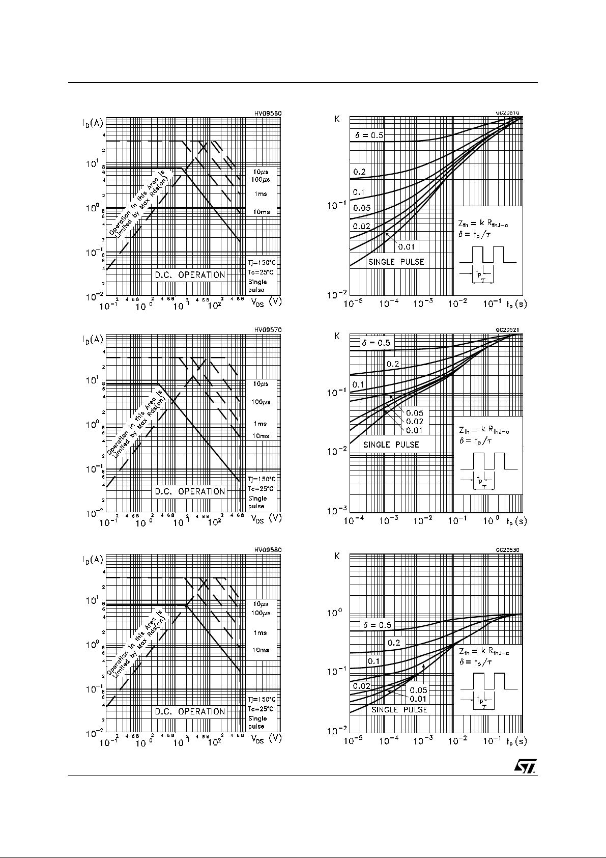
Safe Operating Area For TO-220/D2PAK/I2PAK
Safe Operating Area For TO-220FP
Thermal Impedance For TO-220/D2PAK/I2PAK
Thermal Impedance For TO-220FP
Safe Operating Area For TO-247
4/14
Thermal Impedance For TO - 24 7

STP9NK70Z / STP9NK70ZFP / STB9NK70Z / STB9NK70Z-1 / STW9NK70Z
Output Characteristics
Transconductance Static Drain-source On Resistance
Transfer Characteristics
Capacitance VariationsGate Charge vs Gate-source Voltage
5/14
 Loading...