

SGS Thomson Microelectronics STB9NB60 Datasheet
STB9NB60
N - CHANNEL 600V- 0.7Ω -9A-I2PAK/D2PAK
PowerMESH MOSFET
TYPE V
DSS
R
DS(on)
I
D
STB9NB60 600 V < 0.8 Ω 9A
■ TYPICALR
■ EXTREMELYHIGH dv/dt CAPABILITY
■ 100%AVALANCHETESTED
■ VERYLOW INTRINSIC CAPACITANCES
■ GATECHARGE MINIMIZED
DS(on)
= 0.7 Ω
DESCRIPTION
Using the latest high voltage MESH OVERLAY
process, STMicroelectronics has designed an
advanced family of power MOSFETs with
outstanding performances. The new patent
pending strip layout coupled with the Company’s
proprietary edge termination structure, gives the
lowest RDS(on) per area, exceptional avalanche
and dv/dt capabilities and unrivalled gate charge
and switching characteristics.
APPLICATIONS
■ HIGHCURRENT, HIGHSPEEDSWITCHING
■ SWITCHMODE POWER SUPPLIES (SMPS)
■ DC-AC CONVERTERS FOR WELDING
EQUIPMENTANDUNINTERRUPTIBLE
POWERSUPPLIESAND MOTORDRIVE
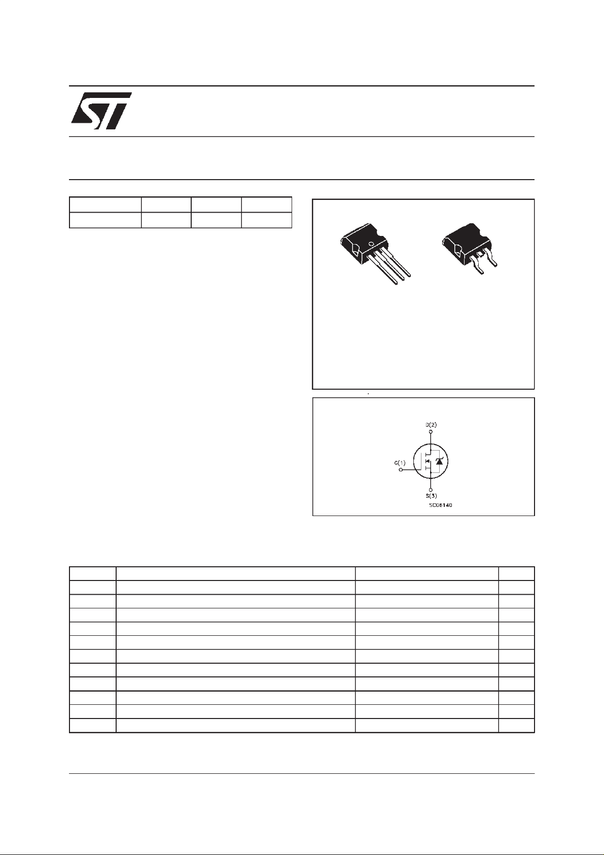
3
1
D2PAK
TO-263
(Suffix ”T4”)
I2PAK
TO-262
(suffix ”-1”)
3
2
1
INTERNAL SCHEMATIC DIAGRAM
ABSOLUTE MAXIMUM RATINGS
Symbol Parameter Value Unit
V
V
V
I
DM
P
dv/dt(
T
(•) Pulse width limited by safe operating area (1)ISD≤ 9A, di/dt ≤ 200 A/µs, VDD≤ V
January 2000
Dra in- sour c e Volt age (VGS= 0) 600 V
DS
Dra in- gat e Volt age (RGS=20kΩ)
DGR
Gat e-source Voltage ± 30 V
GS
Dra in Cu rr ent (cont inuous) at Tc=25oC9A
I
D
Dra in Cu rr ent (cont inuous) at Tc=100oC5.7A
I
D
600 V
(•) Dra in Cu rr ent (pulsed) 36 A
Tot al Dissipat ion at Tc=25oC 125 W
tot
Derating Factor 1 W/
1) Peak Diode Recovery volt age sl ope 4.5 V/ns
St orage Tempe rat ure -65 to 150
stg
Max. Operating Junction Temperat ur e 150
T
j
(BR)DSS
,Tj≤T
JMAX
o
C
o
C
o
C
1/8

STB9NB60
THERMAL DATA
R
thj-case
Rthj-a mb
R
thc-sink
T
AVALANCHE CHARACTERISTICS
Symbol Parameter Max V alue Unit
I
AR
E
Ther mal Res istance Junct ion-case Max
Ther mal Res istance Junct ion-ambient Max
Ther mal Res istance C as e -s ink Ty p
Maximum Lead Temperature For So ldering Purpos e
l
Avalanche Current, Repetitive or Not-Repetitive
(pulse width limited by T
Single Pul s e Avalanc he E ner gy
AS
(starting T
=25oC, ID=IAR,VDD=50V)
j
max)
j
1
62.5
0.5
300
9A
850 mJ
o
C/W
oC/W
o
C/W
o
C
ELECTRICAL CHARACTERISTICS (T
=25oC unless otherwisespecified)
case
OFF
Symbol Parameter Test Conditions Min. Typ. Max. Unit
V
(BR)DSS
Drain-source
=250µAVGS=0
I
D
600 V
Break dow n Voltage
I
DSS
I
GSS
Zero Gate Voltage
Drain Current (V
GS
Gat e- bod y Leak ag e
Current (V
DS
=0)
=0)
V
=MaxRating
DS
=MaxRating Tc=125oC
V
DS
= ± 30 V
V
GS
1
50
± 100 nA
ON(∗)
Symbol Parameter Test Conditions Min. Typ. Max. Unit
V
GS(th)
R
DS(on)
Gate Threshold Voltage
Sta t ic Drain-s ource On
V
DS=VGSID
= 250 µA
VGS=10V ID=3A 0.7 0.8
345V
Resistance
I
D(on)
On State Drain Current VDS>I
D(on)xRDS(on)max
9A
VGS=10V
DYNAMIC
Symbol Parameter Test Conditions Min. Typ. Max. Unit
g
(∗)Forward
fs
Tr ansc on duc tance
C
C
C
Input Capaci t anc e
iss
Out put Capac it ance
oss
Reverse Transfer
rss
Capacit a nc e
VDS>I
D(on)xRDS(on)maxID
=4.5 A 3 6.5 S
VDS=25V f=1MHz VGS= 0 1480
210
25
1924
273
33
µA
µ
Ω
pF
pF
pF
A
2/8
STB9NB60
ELECTRICAL CHARACTERISTICS
(continued)
SWITCHINGON
Symbol Parameter Test Conditions Min. Typ. Max. Unit
t
d(on)
Turn-on Time
r
Rise Tim e
t
VDD=300V ID= 4.5 A
R
=4.7
G
Ω
VGS=10V
25
11
35
15
(see test circuit, figure 3)
Q
Q
Q
Tot al Gate Charge
g
Gat e- Source Charg e
gs
Gate-Drain Charge
gd
VDD= 480 V ID=9 A VGS=10V 40
10.5
17.5
56 nC
SWITCHINGOFF
Symbol Parameter Test Conditions Min. Typ. Max. Unit
t
r(Voff)
t
t
Off-voltage Rise Time
Fall T ime
f
Cross-over Time
c
VDD=480V ID=9 A
=4.7 ΩVGS=10V
R
G
12
10
21
17
14
29
SOURCEDRAINDIODE
Symbol Parameter Test Conditions Min. Typ. Max. Unit
I
SD
I
SDM
V
SD
t
Q
I
RRM
(∗) Pulsed: Pulse duration = 300 µs, duty cycle 1.5 %
(•) Pulse width limited by safe operatingarea
Source-drain Current
(•)
Source-drain Current
9
36
(pulsed)
(∗)ForwardOnVoltage ISD=9A VGS=0 1.6 V
Reverse Recovery
rr
Time
Reverse Recovery
rr
=9A di/dt=100A/µs
I
SD
= 100 V Tj=150oC
V
DD
600
5.4
Charge
Reverse Recovery
18
Current
ns
ns
nC
nC
ns
ns
ns
A
A
ns
µ
A
C
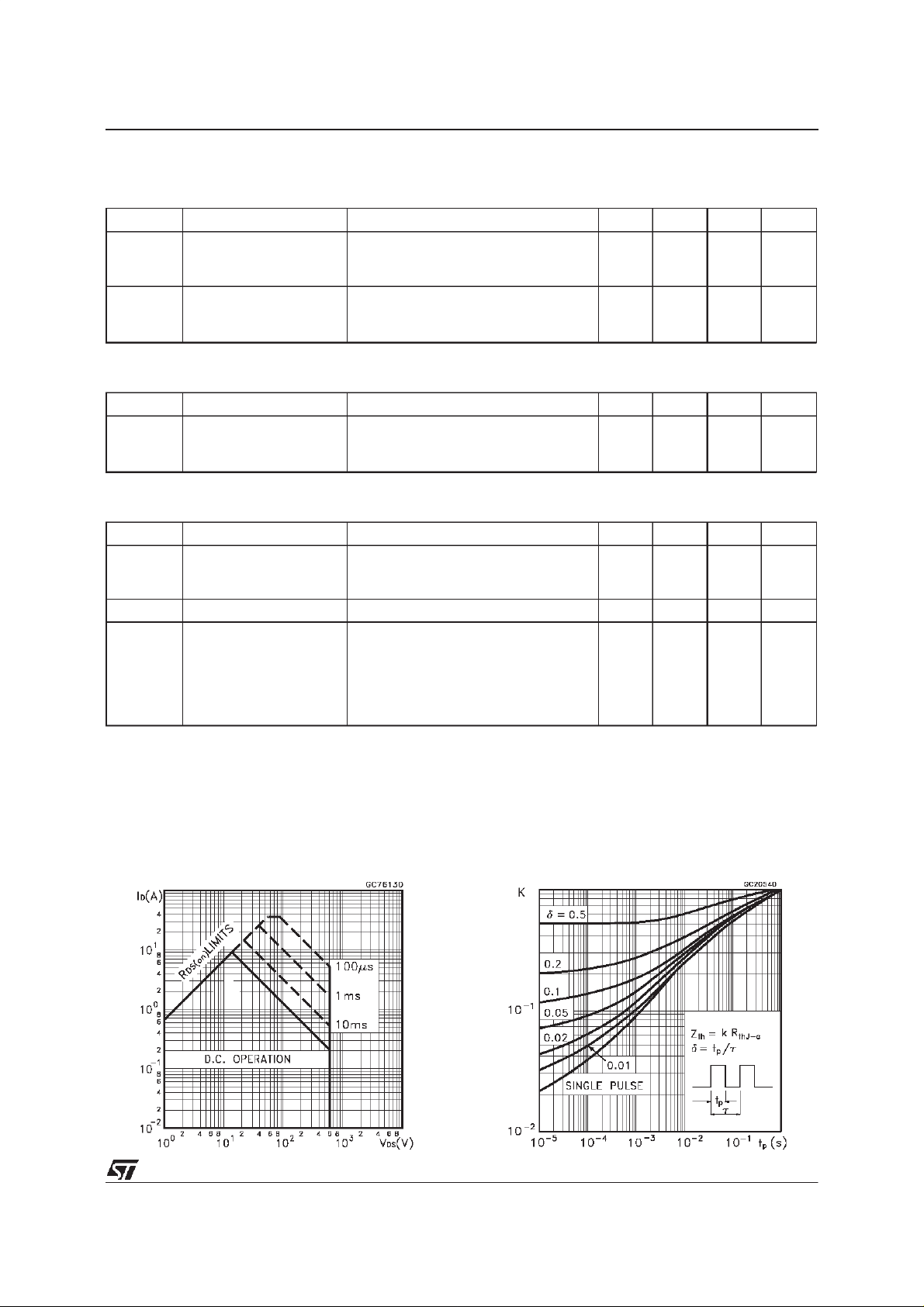
SafeOperating Area ThermalImpedance
3/8
 Loading...