

SGS Thomson Microelectronics STB80NE03L-06 Datasheet
STB80NE03L-06
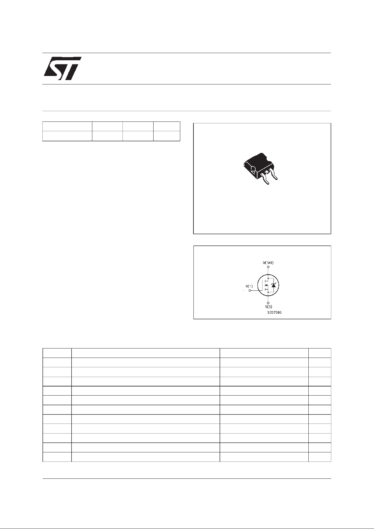
N - CHANNEL 30V - 0.005Ω - 80A - D2PAK
STripFET POWER MOSFET
TYPE V
DSS
R
DS(on)
I
D
STB80NE03L-06 30 V < 0.006 Ω 80 A
■ TYPICALR
■ EXCEPTIONALdv/dt CAPABILITY
■ 100% AVALANCHETESTED
■ LOW GATE CHARGE 100
■ APPLICATIONORIENTED
DS(on)
=0.005 Ω
o
C
CHARACTERIZATION
■ FOR THROUGH-HOLE VERSIONCONTACT
SALESOFFICE
DESCRIPTION
This Power Mosfet is the latest development of
SGS-THOMSON unique ”Single Feature Size”
strip-based process. The resulting transistor
shows extremely high packing density for low
on-resistance, rugged avalance characteristics
and less critical alignment steps therefore a
remarkablemanufacturingreproducibility.
APPLICATIONS
■ HIGH CURRENT, HIGH SPEED SWITCHING
■ SOLENOIDANDRELAY DRIVERS
■ MOTORCONTROL, AUDIOAMPLIFIERS
■ DC-DC& DC-AC CONVERTERS
■ AUTOMOTIVE ENVIRONMENT(INJECTION,
ABS, AIR-BAG,LAMPDRIVERS, Etc. )
3
1
D2PAK
TO-263
(suffix ”T4”)
INTERNAL SCHEMATIC DIAGRAM
ABSOLUTE MAXIMUM RATINGS
Symb o l Para meter Value Uni t
V
V
V
I
DM
P
dv/ dt Peak Diode Recover y volt age slope 7 V/ns
T
(•) Pulsewidth limitedby safe operating area (1)ISD≤ 80 A,di/dt ≤ 300A/µs, VDD≤ V
July 1998
Drain-source Voltage (VGS=0) 30 V
DS
Drain- gate Voltage ( RGS=20kΩ)
DGR
Gat e- source Volt age ± 22 V
GS
I
Drain Current (cont inuous) at Tc=25oC80A
D
I
Drain Current (cont inuous) at Tc=100oC60A
D
30 V
(•) Drain Current (pulsed) 320 A
Tot al Dissipat i on at Tc=25oC150W
tot
Derat in g Factor 1 W/
Sto rage T em pe r ature -65 to 175
stg
T
Max. Operat in g Junct ion Te m peratu re 175
j
(BR)DSS,Tj≤TJMAX
o
C
o
C
o
C
1/8
STB80NE03L-06
THERMAL DATA
R
thj-case
Rthj-a mb
R
thc-sin k
T
AVALANCHE CHARACTERISTICS
Symbol Para met e r Max Va lue Uni t
I
AR
E
Ther mal Res ist ance J unctio n-c a s e Max
Ther mal Res ist ance J unctio n-ambient Max
Ther mal Res ist ance C ase-sink Ty p
Maximum Lead Te mpera t u re For S old eri ng Pur p os e
l
Avalanche Curre nt , Repet it i v e or Not -Repet it ive
(pulse w idth limited by T
Single Pulse Avalanche Energy
AS
(starting T
=25oC, ID=IAR,VDD=15V)
j
max, δ <1%)
j
1
62.5
0.5
300
80 A
600 mJ
o
C/W
oC/W
o
C/W
o
C
ELECTRICAL CHARACTERISTICS (T
=25oC unlessotherwisespecified)
case
OFF
Symbol Parameter Test Cond itions Min. Typ. Max. Unit
V
(BR)DSS
Drain-sourc e
=250µAVGS=0
I
D
30 V
Breakdown Voltage
I
DSS
I
GSS
Zer o Gate Vo ltage
Drain Cur rent (V
GS
Gat e-body Leakage
Current (V
DS
=0)
=0)
=MaxRating
V
DS
V
=MaxRating Tc=125oC
DS
= ± 15 V
V
GS
1
10
± 100 nA
ON (∗)
Symbol Parameter Test Cond itions Min. Typ. Max. Unit
V
GS(th )
Gate Threshold
V
DS=VGSID
=250µA
11.72.5V
Voltage
R
DS(on)
I
D(on)
Stati c Drain-so urce On
Resistance
VGS=10V ID=40A
=5V ID=40A
V
GS
On State Drain Cur rent VDS>I
D(on)xRDS(on)max
0.005 0. 006
0.008ΩΩ
80 A
VGS=10V
DYNAMIC
Symbol Parameter Test Cond itions Min. Typ. Max. Unit
g
(∗)Forward
fs
Tr ansconductanc e
C
C
C
Input Capacit ance
iss
Out put Capa c itanc e
oss
Reverse Transfer
rss
Capa cit an c e
VDS>I
D(on)xRDS(on)maxID
=40 A 30 50 S
VDS=25V f=1MHz VGS= 0 6500
1500
500
8700
2000
700
µA
µA
pF
pF
pF
2/8
STB80NE03L-06
ELECTRICAL CHARACTERISTICS (continued)
SWITCHINGON
Symbol Parameter Test Cond itions Min. Typ. Max. Unit
t
d(on)
t
r
Turn-on Time
Rise Time
VDD=15V ID=40A
=4.7 Ω VGS=5V
R
G
(see test circuit, figure 3)
Q
Q
Q
Total Gate Charge
g
Gat e-Sour ce Charge
gs
Gate-Drain Charge
gd
VDD=24V ID=80A VGS=5V 95
SWITCHINGOFF
Symbol Parameter Test Cond itions Min. Typ. Max. Unit
t
r(Voff)
t
Of f - voltag e Rise Time
t
Fall Time
f
Cross-ov er Tim e
c
VDD=24V ID=80A
=4.7 Ω VGS=5V
R
G
(see test circuit, figure 5)
SOURCE DRAIN DIODE
Symbol Parameter Test Cond itions Min. Typ. Max. Unit
I
SD
I
SDM
V
SD
t
Q
I
RRM
(∗) Pulsed: Pulse duration =300 µs, duty cycle 1.5 %
(•) Pulse widthlimited by safeoperating area
Source-drain Current
(•)
Source-drain Current
(pulsed)
(∗) For ward O n Voltage ISD=80A VGS=0 1.5 V
Reverse Recovery
rr
Time
Reverse Recovery
rr
= 80 A di/dt = 100 A/µs
I
SD
=15V Tj=150oC
V
DD
(see test circuit, figure 5)
Charge
Reverse Recovery
Current
40
26055350
130 nC
30
44
70
165
250
95
220
340
80
320
75
0.14
4
ns
ns
nC
nC
ns
ns
ns
A
A
ns
µC
A
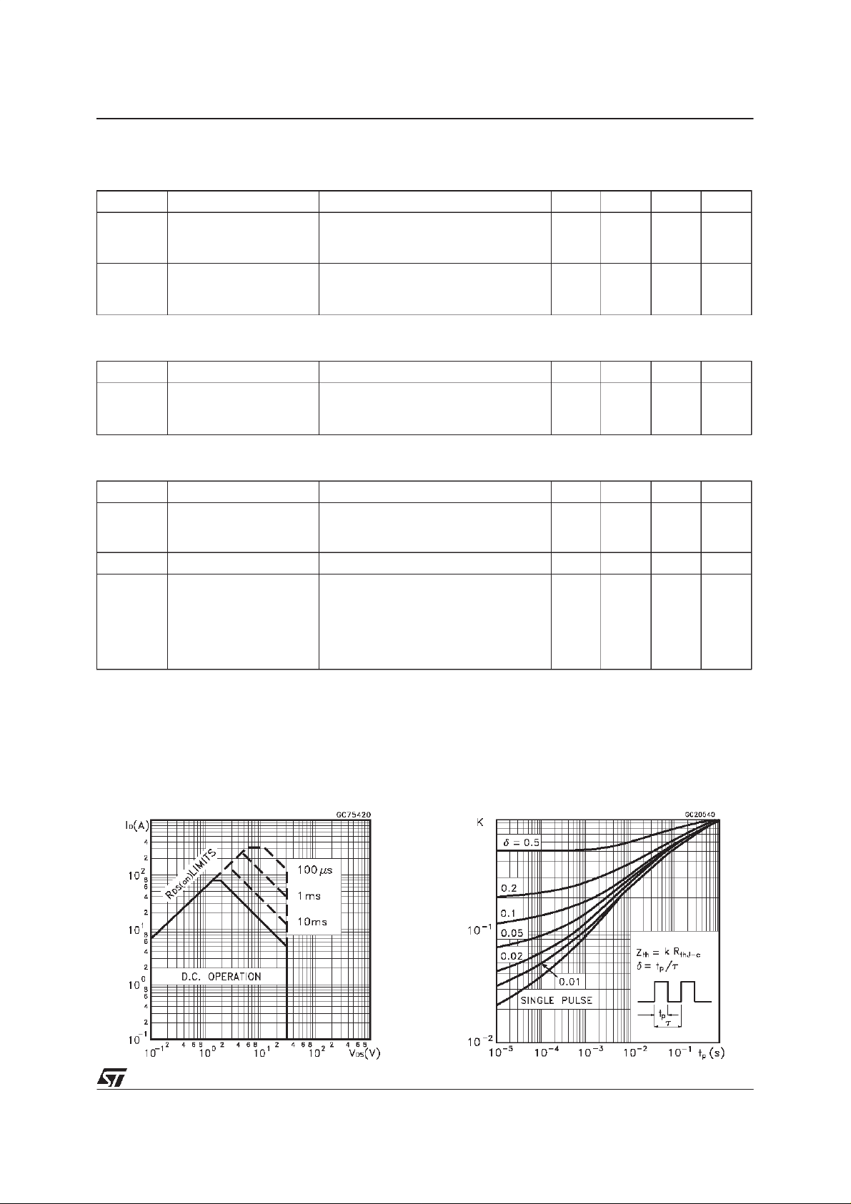
Safe Operating Areafor ThermalImpedance
3/8
 Loading...