

SGS Thomson Microelectronics STB7003 Datasheet
• SUPPLY VOLTAGE 2.8V
S
• LOW CURRENT CONSUMPTION
• VERY LOW NOISE FIGURE:
NF=1.5dB @ 950MHz
NF=1.9dB @ 1850MHz
NF=2dB @ 1950MHz
• DIGITAL GAIN CONTROL
APPLICATIONS
TRI-BAND GSM/DCS/PCS FRONT-ENDS
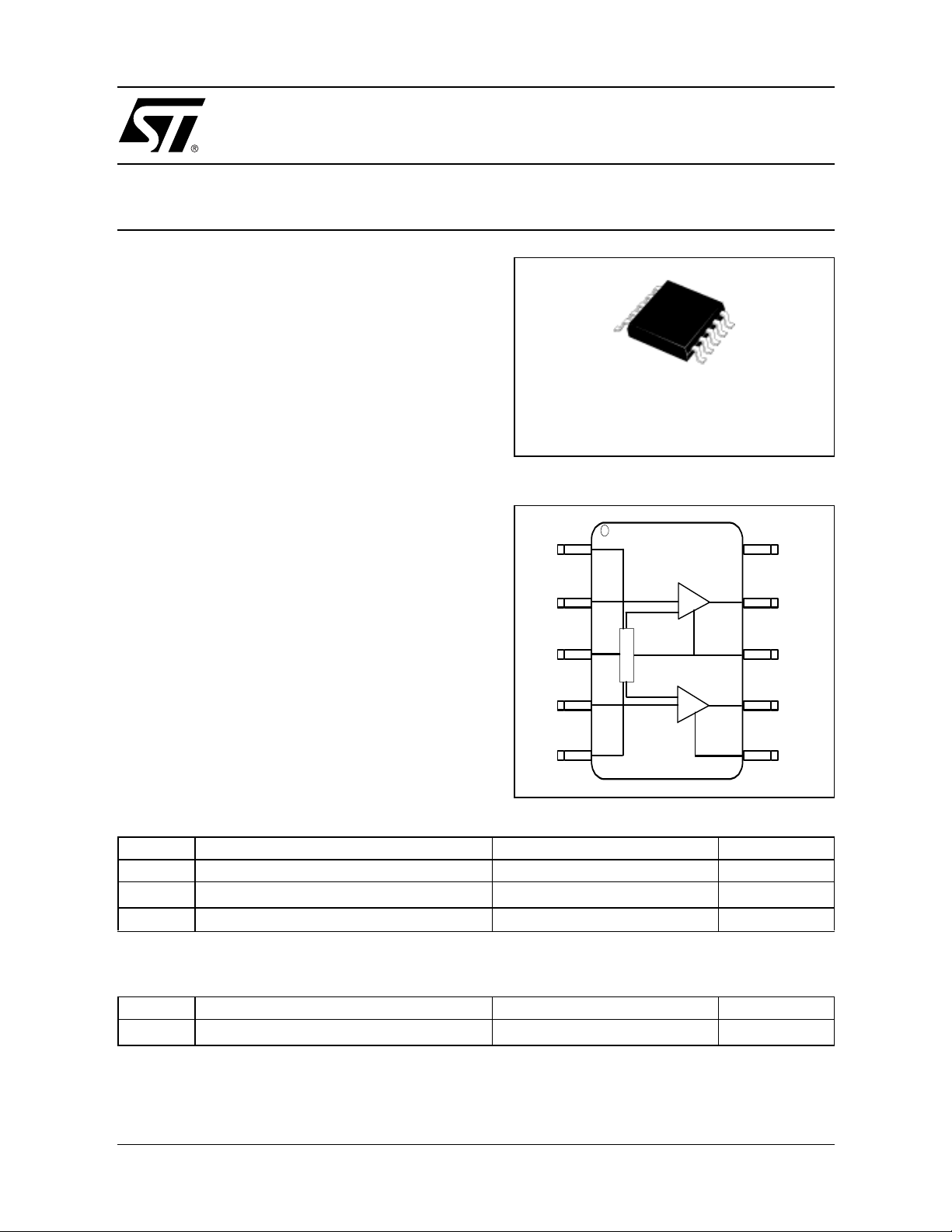
STB7003
TRI-BAND GSM/DCS/PCS LNA
MSOP10-EP
(exposed pad)
ORDER CODE
STB7003
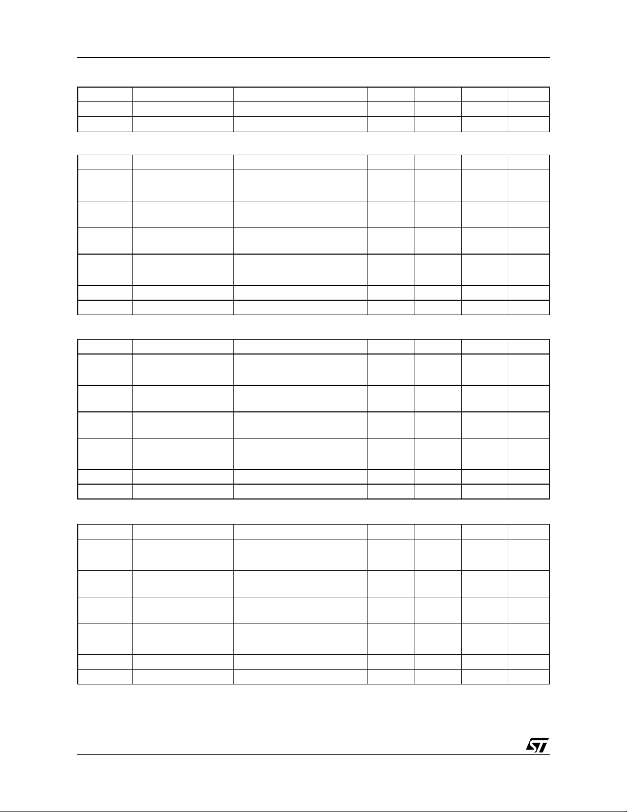
FUNCTIONAL BLOCK DIAGRAM
BRANDING
7003
DESCRIPTION
PD
The STB7003 is a tri-band LNA designed for GSM/DCS/
PCS applications. The GC pin sets the LNA gain levels.
AI1
LNA 1
The innovative architecture implemented allows to
reach very low current consumption. LNA1 works at
0.9-1.0 GHz and LNA2 over the 1.8-2GHz frequency
GND
BIAS
range.
AI2
BSW
LNA2
ABSOLUTE MAXIMUM RATING
Symbol Parameter Value Unit
Vcc Supply voltage 4.5 V
Tj Junction temperature 150
T
stg
Storage temperature -40 to +85 °C
THERMA L D ATA
Symbol Parameter Value Unit
R
th(j-a)
Thermal resistance junction- ambi ent TBD
o
C/W
GC
AO1
GSM
Vcc
AO2
DC
Vcc
o
C
1/9January, 22 2002
STB7003
ELECTRICAL CHARACTERISTICS (Vcc = 2.8V, Tamb= 25 oC)
Symbol Parameter Test conditions Min. Typ. Max. Unit
Vcc Supply voltage 2.7 3.3 V
I
PD
LNA1 @ 950MHz
Icc Supply current 4.5 mA
G Power gain
NF
P1dB
IIP3
VSWRi Input VSWR 2:1
VSWRo Output VSWR 2:1
LNA2 @ 1850MHz
Icc Supply current 7.3 mA
G Power gain
NF Noise figure
P1dB
IIP3
VSWRi Input VSWR 2:1
VSWRo Output VSWR 2:1
Sleep supply current 5 uA
(1)
Noise figure
Input 1 dB compr.
power
Input third order
intercept
Input 1 dB compr.
power
Input third order
intercept
G
p1
(1)
G
p2
G
p1
G
p2
G
p1
G
p2
(2)
G
p1
(2)
G
p2
(1)
G
p1
(1)
G
p2
G
p1
G
p2
G
p1
G
p2
(3)
G
p1
(3)
G
p2
-1
16
5.5
1.5
-19
-21
-10.8
-12.6
-4
14.7
9.6
1.9
-11.5
-13.1
-1.4
-3.5
dB
dB
dBm
dBm
dB
dB
dBm
dBm
LNA2 @ 1950MHz
Icc Supply current 7.3 mA
(1)
G
G Power gain
NF Noise figure
P1dB
IIP3
Input 1 dB compr.
power
Input third order
intercept
p1
(1)
G
p2
G
p1
G
p2
G
p1
G
p2
(4)
G
p1
(4)
G
p2
VSWRi Input VSWR 2:1
VSWRo Output VSWR 2:1
Note(1) : Gp1 min gain, Gp2 max gain.
Note(2) : Measured data with two tones f
Note(3) : Measured data with two tones f
Note(4) : Measured data with two tones f
= 945 MHz, f
IN1
= 1850 MHz, f
IN1
= 1960 MHz, f
IN1
= 945.8 MHz, P
IN2
= 1850.8 MHz, P
IN2
= 1960.8 MHz, P
IN2
= - 33 dBm for each tone
IN
= - 33 dBm fo r each tone
IN
= - 33 dBm fo r each tone
IN
2/9
-4.5
14.7
9.8
2
-10.8
-12.6
-1.5
-3.7
dB
dB
dBm
dBm
GAIN SELECTI ON
BSW GC
0 0 High gain Off
0 1 Low gain Off
1 0 Off High gain
1 1 Off Low gain
GSM
LNA1
DCS/PCS
LNA2
PINOUT
Pin Number Symbol Description
1 PD Power down
2 AI1 GSM LNA1 input
3 GND Ground
4 AI2 DCS/PCSl LNA2 input
5 BSW Band switch between GSM and DCS/PCS RF output
6
7 AO2 DCS/PCS LNA2 output
Vcc
DCS
DCS Supply voltage
STB7003
8
9 AO1 GSM LNA1 output
10 GC LNA1/2 gain control
Vcc
GSM
GSM/BiAS Supply voltage
3/9
 Loading...