SGS Thomson Microelectronics STB7001 Datasheet

900 MHz THREE GAIN LEVEL LNA
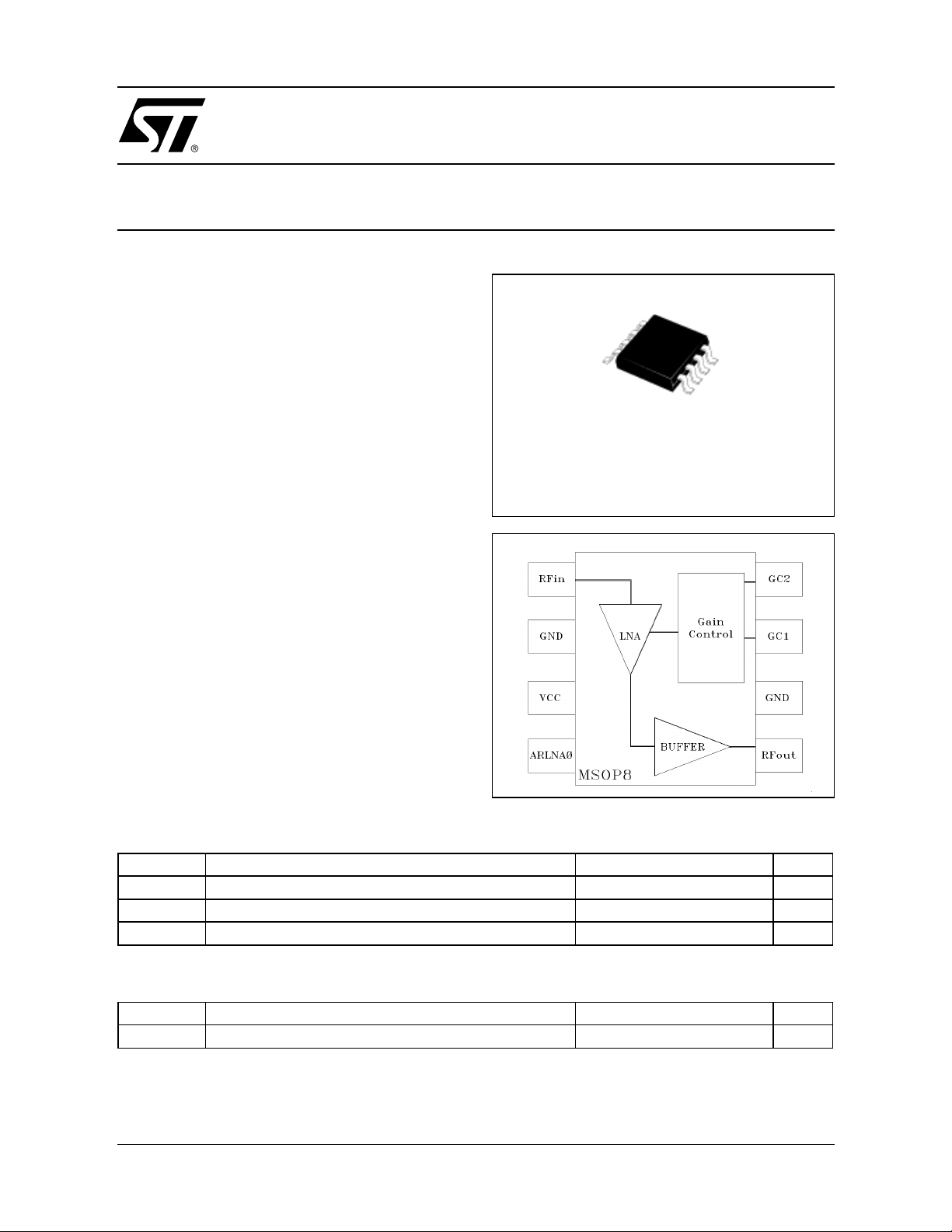
• FULLY INTEGRATED 900 MHz LNA
• THREE GAIN LEVELS (0dB, 18dB, 26dB typ.
@ 2.8V)
• LOW NOISE FIGURE
• TEMPERATURE COM PENSATED
STB7001
APPLICATIONS
MSOP8
• GSM HANDSETS
ORDER CODE
STB7001
BRANDING
7001
DESCRIPTION
The STB7001 is a Silicon monolithic amplifier, that
offers low noise figure and three gain levels for
900-MHz applications. STB7001 is housed in a
small industry-standard MSOP8 surface mount
package, requiring very little board space (50% reduction vs SO8 Package). MSOP8 dimensions
are 3mmx5mm with a 1 .1mm thickness. The device is ESD protected and requires minimum external components in the application circuit, for the
on-chip bias and gain cont rol . Furtherm ore, temperature and supply voltage compensation assures high stability over a wide range of operating
conditions.
ABSOLUTE MAXIMUM RATINGS
Symbol Parameter Value Unit
V
cc
Tj Junction Temperature 150 °C
T
stg
Supply voltage 5.5 V
Storage temperature -40 to +85 °C
THERMA L D ATA
Symbol Parameter Value Unit
R
th(j-a)
Junction -ambient Thermal Resistance 200 °C/W
1/7January, 22 2002

STB7001
ELECTRICAL SPECIFICATION (T
= 25°C, Vcc = 2.8V)
amb
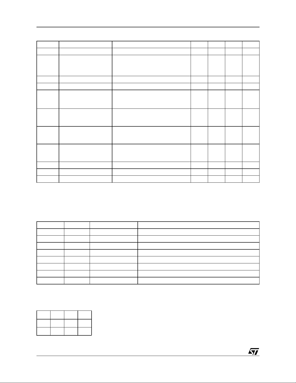
Symbol Parameters Test Conditions Min. Typ. Max. Unit
Vcc Supply voltage 2.7 2.8 2.9 V
(1)
for G
I
bias
Bias current
p1
G
p2
G
p3
(1)
(1)
14
10
8
11.5
17.5
15.0
15.0
22.5
19
Istby Standby current 20 µA
f Frequency range 925 960 MHz
for G
p1
G
p1,2,3
NF
P1dB
IIP3
Power gain
1,2,3
1,2,3
1,2,3
Noise figure
Input 1 dB Compr.Power
Input Third Order Intercept
for G
for G
for G
-3.0
G
p2
16.0
24.0
G
p3
p1
G
p2
G
p3
p1
G
p2
G
p3
p1
G
p2
G
p3
0.0
18.0
26.0
10
3.1
2.5
-15.0
-19.0
-26.5
-6.0
-11.0
-20.0
3.0
20.0
28.0
VSWRi Input VSWR 1.5:1
VSWRo Output VSWR 1.5:1
AZout Zout LNA on/off 15 %
Note(1) : Gp1 min gain, Gp2 mid gain and Gp3 max gain.
mA
dB
dB
dBm
dBm
PINOUT
Pin Number Symbol Description Evaluation circuit components
1 RFin RF input L2 = 5.1nH, C2 = n/c
2 Gnd Ground
3 Vcc Voltage supply C4 = 8pF, L1 = 110nH, C7 = 10nF, C6 = 4.7uF
4 ARLNA0 Enable for power down C3 = 10nF
5 RFout RF output C9 = 5pf, L3 = 10nH, C10 = 10nF, C11 = 100pF, L4 = 110nH
6 Gnd Ground
7 GC1 Gain selection C5 = 10nF
8 GC2 Gain selection C8 = 10nF
GAIN SELECTI 0 N
G
G
p2
G
p3
p1
GC1 001
GC2 011
2/7

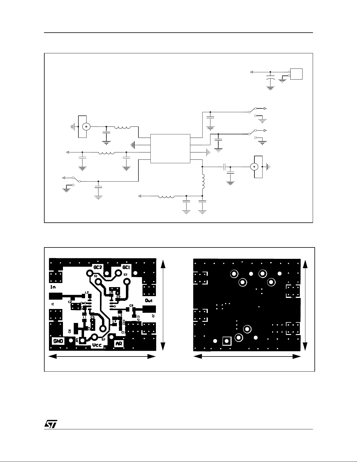
TEST CIRCUIT SCHEMATIC
J1
VCC
VCC
S2
SW_SPDT
SMA_IN
C7
10n
L1
110n
C3
10n
C2
n/c
5n1
STB7001
JP1
VCC
C8
C10
10n
10n
C5
10n
C9
5p
L2
U1
C4
8p
VCC
1
RF_IN
2
GND
3
VCC
ARLNA04RF_OUT
LNA
STB7001
L4
110n
GC2
GC1
GND
C11
100p
8
7
6
5
L3
10n
SW SPDT
SW SPDT
SMA_OUT
C12
n/c
C6
4u7
S1
VCC
S3
VCC
J2
1
2
BIAS
TEST CIRCUIT PHOTOMASTER (board dimenti ons 23.5x20. 3m m)
TOP VIEW
20.3mm
23.5mm
BOTTOM VIEW
20.3mm
23.5mm
3/7
 Loading...