

SGS Thomson Microelectronics STB6NB90 Datasheet
®
N - CHANNEL 900V - 1.7Ω - 5.8A - D2PAK
TYPE V
DSS
STB6NB90 900 V < 2.0 Ω 5.8 A
■
TYPICAL R
■
EXTREMELY HIGH dv/dt CAPABILITY
■
100% AVALANCHE TESTED
■
VERY LOW INTRINSIC CAPACITANCES
■
GATE CHARGE MINIMIZED
■
ADD SUFFIX "T4" FOR ORDERING IN TAPE
DS(on)
= 1.7
& REEL (500 UNITS)
DESCRIPTION
Using the latest high voltage MESH OVERLAY
process, STMicroelectronics has designed an
advanced family of power MOSFETs with
outstanding performances. The new patent
pending strip layout coupled with the Company’s
proprietary edge termination structure, gives the
lowest RDS(on) per area, exceptional avalanche
and dv/dt capabilities and unrivalled gate charge
and switching characteristics.
R
DS(on)
I
D
Ω
STB6NB90
PowerMESH MOSFET
PRELIMINARY DATA
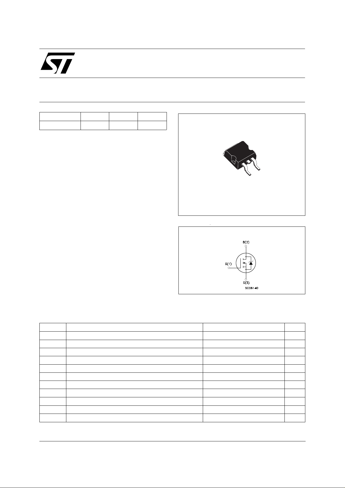
D2PAK
TO-263
INTERNAL SCHEMATIC DIAGRAM
APPLICATIONS
■
HIGH CURRENT, HIGH SPEED SWITCH ING
■
SWITCH MODE POWER SUPPLIES (SMPS)
■
DC-AC CONVERTERS FOR WELDING
EQUIPMENT AND UNINTERRUPTI BLE
POWER SUPPLIES AND MOTOR DRIVE
ABSOLUTE MAXIMUM RATINGS
Symbol Parameter Value Unit
V
V
V
I
DM
P
dv/dt(
T
(•) Limited only by maximum temperature allowed (1) ISD ≤ 6 A, di/dt ≤ 200 A/µs, VDD ≤ V
Drain-source Voltage (VGS = 0) 900 V
DS
Drain- gate Voltage (RGS = 20 kΩ)
DGR
Gate-source Voltage ± 30 V
GS
Drain Current (continuous) at Tc = 25 oC 5.8 A
I
D
Drain Current (continuous) at Tc = 100 oC 3.6 A
I
D
900 V
(•) Drain Current (pulsed) 23 A
Total Dissipation at Tc = 25 oC 135 W
tot
Derating Factor 1.08 W/
) Peak Diode Recovery voltage slope 4.5 V/ns
1
Storage Temperature -65 to 150
stg
Max. Operating Junction Temperature 150
T
j
, Tj ≤ T
(BR)DSS
JMAX
o
C
o
C
o
C
February 1999
1/5
STB6NB90
THERMAL DATA
R
thj-case
Rthj-am b
R
thc-sink
T
Thermal Resistance Junction-case Max
Thermal Resistance Junction-ambient Max
Thermal Resistance Case-sink Typ
Maximum Lead Temperature For Soldering Purpose
l
AVALANCHE CHARACTERIST ICS
Symbol Parameter Max Value Unit
I
AR
E
Avalanche Current, Repetitive or Not-Repetitive
(pulse width limited by T
Single Pulse Avalanche Energy
AS
(starting T
= 25 oC, ID = IAR, V
j
max)
j
DD
= 50 V)
0.92
62.5
0.5
300
5.8 A
750 mJ
o
C/W
oC/W
o
C/W
o
C
ELECTRICAL CHARACTERISTICS
= 25 oC unless otherwise specified)
(T
case
OFF
Symbol Parameter Test Conditions Min. Typ. Max. Unit
V
(BR)DSS
Drain-source
I
= 250 µA V
D
GS
= 0
900 V
Breakdown Voltage
I
DSS
I
GSS
Zero Gate Voltage
Drain Current (V
GS
Gate-body Leakage
Current (V
DS
= 0)
= 0)
= Max Rating
V
DS
V
= Max Rating Tc = 125 oC
DS
V
= ± 30 V
GS
1
50
± 100 nA
ON (∗)
Symbol Parameter Test Conditions Min. Typ. Max. Unit
V
GS(th)
Gate Threshold
V
= VGS ID = 250 µA
DS
345V
Voltage
R
DS(on)
Static Drain-source On
VGS = 10V ID = 3 A 1.7 2 Ω
Resistance
I
D(on)
On State Drain Current VDS > I
V
= 10 V
GS
D(on)
x R
DS(on)max
5.8 A
DYNAMIC
Symbol Parameter Test Conditions Min. Typ. Max. Unit
g
(∗) Forward
fs
Transconductance
C
C
C
Input Capacitance
iss
Output Capacitance
oss
Reverse Transfer
rss
Capacitance
VDS > I
V
DS
x R
D(on)
DS(on)max
= 25 V f = 1 MHz V
ID = 3 A 1.5 6 S
= 0 1400
GS
160
18
µA
µA
pF
pF
pF
2/5
 Loading...