

STB60N03L-10
N - CHANNEL ENHANCEMENT MODE
POWER MOS TRANSISTOR
PRELIMIRARY DATA
■ TYPICAL R
DS(on)
= 0.0085 Ω
■ AVALANCHE RUGGED TECHNOLOGY
■ 100% AVALANCHE TESTED
■ REPETITIVE AVA LANCHE DATA AT 100
o
C
■ LOW GATE CHARGE
■ HIGH CURRENT CAPABILITY
■ 175
o
C OPERATING TEMPERATURE
■ APPLICATION ORIENTED
CHARACTERIZATION
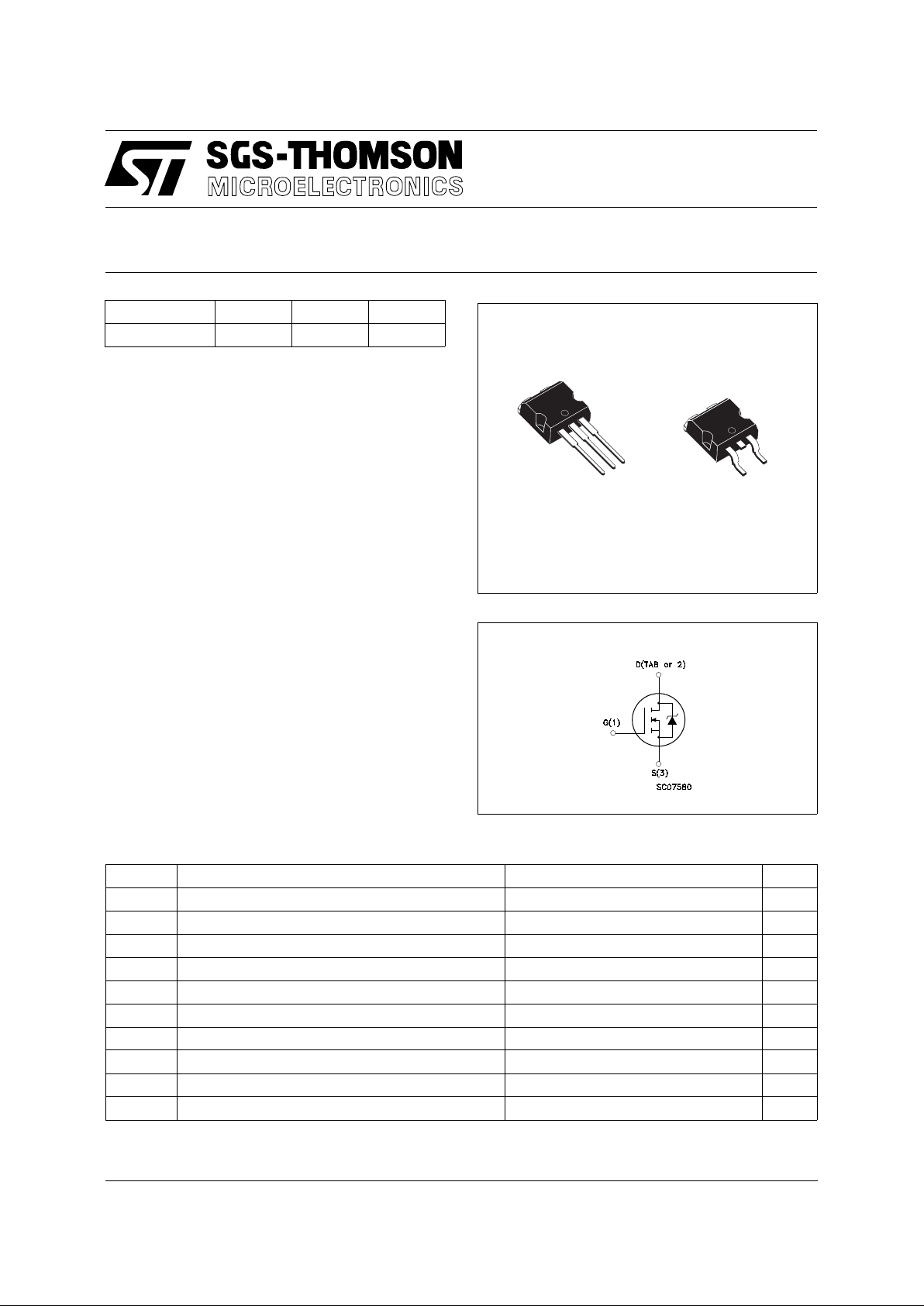
■ THROUGH-HO LE I2PAK (TO -262) POWE R
PACKAGE IN TU BE (SUFFIX "-1")
■ SURFACE-MOUNTING D2PACK (TO-263)
POWER PACKAGE IN TUBE (NO SUFFIX)
OR IN TAPE & REEL (SUFFIX "T4")
APPLICATIONS
■ HIGH CURRENT, HIGH SPE ED SWI TCHING
■ SOLENOID AND RELAY DRIVER S
■ REGULAT O RS
■ DC-DC & DC-AC CONVERT E RS
■ AUTOMOTIVE ENVIRONMENT (INJECTION,
ABS, AIR-BAG, LAMPDRIVERS, Etc.)
INTERNAL SCHEMATIC DIAGRAM
ABSOL UT E MAXIMU M RATINGS
Symbol Parameter Value Unit
V
DS
Drain-source Voltage (VGS = 0) 30 V
V
DGR
Drain- gate Voltage (RGS = 20 kΩ)30V
V
GS
Gate-source Voltage ± 20 V
I
D
Drain Current (continuous) at Tc = 25 oC60A
I
D
Drain Current (continuous) at Tc = 100 oC42A
I
DM
(•) Drain Current (pulsed) 240 A
P
tot
Total Dissipation at Tc = 25 oC 150 W
Derating Factor 1 W/
o
C
T
stg
Storage Temperature -65 to 175
o
C
T
j
Max. Operating Junction Temperature 175
o
C
(•) Pulse width limited by safe operating area
March 1996
TYPE V
DSS
R
DS(on)
I
D
STB60N03L-10 30 V < 0.01 Ω 60 A
1
2
3
1
3
I2PAK
TO-262
D2PAK
TO-263
1/6
THERMAL DATA
R
thj-case
R
thj-amb
R
thj-amb
T
l
Thermal Resistance Junction-case Max
Thermal Resistance Junction-ambient Max
Thermal Resistance Case-sink Typ
Maximum Lead Temperature For Soldering Purpose
1
62.5
0.5
300
o
C/W
o
C/W
o
C/W
o
C
AVALANCHE CHARACTERI S TICS
Symbol Parameter Max Value Unit
I
AR
Avalanche Current, Repetitive or Not-Repetitive
(pulse width limited by T
j
max, δ < 1%)
60 A
E
AS
Single Pulse Avalanche Energy
(starting T
j
= 25 oC, ID = IAR, V
DD
= 25 V)
600 mJ
E
AR
Repetitive Avalanche Energy
(pulse width limited by T
j
max, δ < 1%)
150 mJ
I
AR
Avalanche Current, Repetitive or Not-Repetitive
(T
c
= 100 oC, pulse width limited by Tj max, δ < 1%)
42 A
ELECTRICAL CHARACTERISTICS (T
case
= 25 oC unless otherwise specified)
OFF
Symbol Parameter Test Conditions Min. Typ. Max. Unit
V
(BR)DSS
Drain-source
Breakdown Voltage
ID = 250 µA V
GS
= 0 30 V
I
DSS
Zero Gate Voltage
Drain Current (V
GS
= 0)
V
DS
= Max Rating
V
DS
= Max Rating x 0.8 Tc = 125 oC
250
1000µAµA
I
GSS
Gate-body Leakage
Current (V
DS
= 0)
V
GS
= ± 20 V ± 100 nA
ON (∗)
Symbol Parameter Test Conditions Min. Typ. Max. Unit
V
GS(th)
Gate Threshold Voltage V
DS
= VGS ID = 250 µA 1 1.7 2.5 V
R
DS(on)
Static Drain-source On
Resistance
VGS = 10 V ID = 30 A
V
GS
= 10 V ID = 30 A Tc = 100 oC
V
GS
= 5 V ID = 30 A Tc = 25 oC
V
GS
= 5 V ID = 30 A Tc = 100 oC
0.0085
0.0012
0.01
0.02
0.015
0.03
Ω
Ω
Ω
Ω
I
D(on)
On State Drain Current VDS > I
D(on)
x R
DS(on)max
V
GS
= 10 V
60 A
DYNAMIC
Symbol Parameter Test Conditions Min. Typ. Max. Unit
g
fs
(∗) Forward
Transconductance
VDS > I
D(on)
x R
DS(on)max
ID = 30 A 30 50 S
C
iss
C
oss
C
rss
Input Capacitance
Output Capacitance
Reverse Transfer
Capacitance
V
DS
= 25 V f = 1 MHz V
GS
= 0 3500
1200
450
pF
pF
pF
STB60N03L-10
2/6
 Loading...