

SGS Thomson Microelectronics STP5NC70ZFP, STP5NC70Z, STB5NC70Z-1, STB5NC70Z Datasheet
STP5NC70Z - STP5NC70ZFP
STB5NC70Z - STB5NC70Z-1
N-CHANNEL 700V - 1.8Ω - 4.6A TO-220/FP/D²PAK/I²PAK
Zener-Protected PowerMESH™III MOSFET
TYPE V
DSS
R
DS(on)
I
D
STP5NC70Z/FP 700V < 2 Ω 4.6 A
STB5NC70Z/-1 700V < 2 Ω 4.6 A
■ TYPICAL R
■ EXTREMELY HIGHdv/dtAND CAPABILITYGATE
(on) = 1.8 Ω
DS
TO - SOURCE ZENER DIODES
■ 100% AVALANCHE TESTED
■ V ER Y LOW GATE INPUT RESISTANCE
■ GAT E CHARGE MINIMIZED
DESCRIPTION
The third generation of MESH OVERLAY™ Power
MOSFETs for very high voltage exhibits unsurpassed
on-resistance per unit area while integrating back-toback Zenerdiodes between gate andsource. Such arrangement gives extra ESD capability with higher ruggedness performance as requested by a large variety
of single-switch applications.
APPLICATIONS
■ S INGLE -ENDED S MPS IN MONITORS,
COMPUTER AND INDUSTRIALAPPLICATION
■ WELDING EQUIPMENT
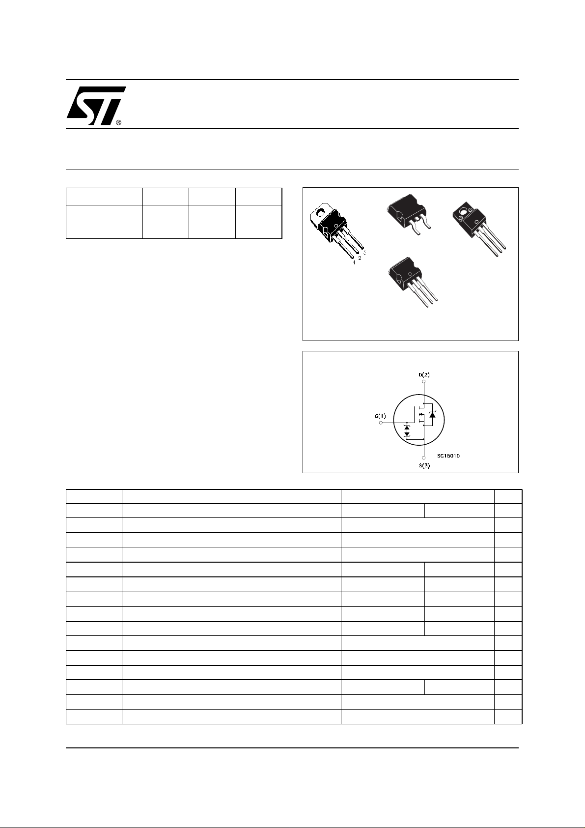
3
1
D²PAK
TO-220
1
3
2
TO-220FP
I²PAK
(Tabless TO-220)
INTERNAL SCHEMATIC DIAGRAM
3
2
1
ABSOLUTE MAXIMUM RATINGS
Symbol Parameter Value Unit
STP(B)5NC70Z(-1) STP5NC70ZFP
V
DS
V
DGR
V
GS
I
D
I
D
I
DM
P
TOT
I
GS
V
ESD(G-S)
dv/dt Peak Diode Recovery voltage slope 3 V/ns
V
ISO
T
stg
T
(1)Pulse width limited by safe operating area
Drain-source Voltage (VGS=0)
Drain-gate Voltage (RGS=20kΩ)
700 V
700 V
Gate- source Voltage ± 25 V
Drain Current (continuous) at TC= 25°C
Drain Current (continuous) at TC= 100°C
(1)
Drain Current (pulsed) 18.4 18.4 A
Total Dissipation at TC= 25°C
4.6 4.6(*) A
2.9 2.9(*) A
100 35 W
Derating Factor 0.8 0.32 W/°C
Gate-source Current ± 50 mA
Gate source ESD(HBM-C=100pF, R=15KΩ) 3KV
Insulation Winthstand Voltage (DC) -- 2000 V
Storage Temperature –65 to 150 °C
Max. Operating Junction Temperature 150 °C
j
(●)ISD≤4.5A, di/dt ≤100A/µs, VDD≤ V
(*).Limited only by maximum temperature allowed
(BR)DSS,Tj≤TJMAX
1/12December 2002
STP5NC70Z - STP5NC70ZFP - STB5NC70Z - ST B 5NC70Z -1
THERMAL DATA
TO-220 / D²PAK
I²PAK
Rthj-case Thermal Resistance Junction-case Max 1.25 3.57 °C/W
Rthj-amb Thermal Resistance Junction-ambient Max 62 °C/W
T
Maximum Lead Temperature For Soldering Purpose 300 °C
l
AVALANCHE CHARACTERISTICS
Symbol Parameter Max Value Unit
I
AR
E
AS
Avalanche Current, Repetitive or Not-Repetitive
(pulse width limited by T
max)
j
Single Pulse Avalanche Energy
(starting T
= 25 °C, ID=IAR,VDD=50V)
j
ELECTRICAL CHARACTERISTICS (TCASE = 25 °C UNLESS OTHERWISE SPECIFIED)
OFF
Symbol Parameter Test Conditions Min. Typ. Max. Unit
V
∆BV
(BR)DSS
Drain-source
Breakdown Voltage
/∆TJBreakdown Voltage Temp.
DSS
Coefficient
I
DSS
Zero Gate Voltage
Drain Current (V
I
GSS
Gate-body Leakage
Current (V
DS
=0)
GS
=0)
ID= 250 µA, VGS= 0 700 V
ID=1mA,VGS= 0 0.8 V/°C
V
= Max Rating
DS
= Max Rating, TC= 125 °C
V
DS
V
= ± 20V ±10 µA
GS
TO-220FP
4.6 A
200 mJ
1µA
50 µA
ON (1)
Symbol Parameter Test Conditions Min. Typ. Max. Unit
V
GS(th)
R
DS(on)
Gate Threshold Voltage
Static Drain-source On
V
DS=VGS,ID
VGS=10V,ID= 2.4 A
= 250µA
345V
1.8 2.0 Ω
Resistance
DYNAMIC
Symbol Parameter Test Conditions Min. Typ. Max. Unit
(1) Forward Transconductance VDS>I
g
fs
C
iss
C
oss
C
rss
Input Capacitance
Output Capacitance 98 pF
Reverse Transfer
Capacitance
D(on)xRDS(on)max,
ID= 2.4A
V
=25V,f=1MHz,VGS=0
DS
4S
1200 pF
9pF
2/12
STP5NC70Z - STP5NC70ZFP - STB5NC70Z - STB5NC70Z-1
ELECTRICAL CHARACTERISTICS (CONTINUED)
SWITCHING ON
Symbol Parameter Test Conditions Min. Typ. Max. Unit
t
d(on)
Q
Q
Q
t
r
g
gs
gd
Turn-on Delay Time
Rise Time
Total Gate Charge
Gate-Source Charge 8 nC
Gate-Drain Charge 10 nC
SWITCHING OFF
Symbol Parameter Test Conditions Min. Typ. Max. Unit
t
r(Voff)
t
t
f
c
Off-voltage Rise Time
Fall Time 14 ns
Cross-over Time 22 ns
SOURCE DRAIN DIODE
Symbol Parameter Test Conditions Min. Typ. Max. Unit
I
SDM
V
I
SD
Q
I
RRM
SD
t
rr
rr
Source-drain Current 4.6 A
(2)
Source-drain Current (pulsed) 18.4 A
(1)
Forward On Voltage
Reverse Recovery Time
Reverse Recovery Charge 4.4 µC
Reverse Recovery Current 15.5 A
VDD=350V,ID= 2.5 A
RG= 4.7Ω VGS=10V
(see test circuit, Figure 3)
V
=560V,ID= 5A,
DD
V
=10V
GS
V
= 560V, ID=5A,
DD
RG=4.7Ω, VGS= 10V
(see test circuit, Figure 5)
ISD= 4.6 A, VGS=0
I
= 5 A, di/dt= 100A/µs, V
SD
= 100V, Tj= 150°C
(see test circuit, Figure 5)
DD
22
10
27 36.4 nC
13 ns
1.6 V
570 ns
ns
ns
GATE-SOURCE ZENER DIODE
Symbol Parameter Test Conditions Min. Typ. Max. Unit
BV
GSO
Gate-Source Breakdown
Igs=± 1mA (Open Drain) 25 V
Voltage
αT Voltage Thermal Coefficient T=25°C Note(3) 1.3
I
Rz Dynamic Resistance
Note: 1. Pulsed: Pulse duration = 300 µs, duty cycle 1.5 %.
2. Pulse width limited by safe operating area.
3. ∆V
= αT(25°-T)BV
BV
GSO
(25°)
=50mA,VGS=0
D
90 Ω
10
-4
/°C
PROTECTION FEATURES OF GATE-TO-SOURCE ZENER DIODES
The built-inback-to-back Zener diodesha ve specifically beendesigned toenhance not onlythe device’s
ESD capability, but also to make them saf ely absorb possible voltage transients that may occasionally
be appliedfrom gate to source.In this r es pec t the Zenervoltage is appropiateto achieve anefficient and
cost-effective intervention toprotect the device’s integrity. These integrated Zener diodes thusavoid the
usage of external components.
3/12
STP5NC70Z - STP5NC70ZFP - STB5NC70Z - ST B 5NC70Z -1
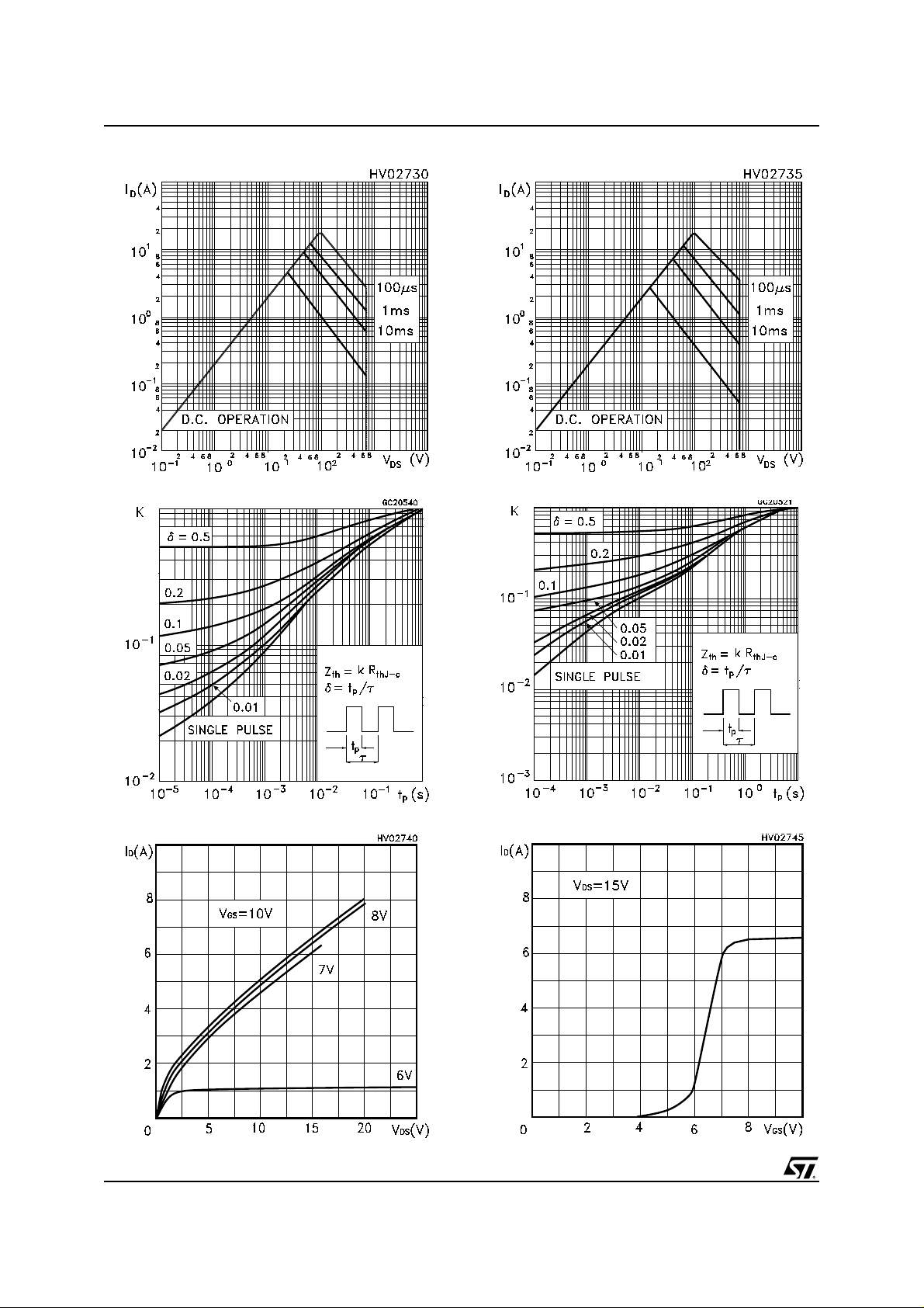
Safe Operating Area For TO-220FPSafe Operating Area For TO-220/D²PAK/I²PA K
Thermal Impedance For TO-220/D²PAK/I²PA K Thermal Impedance For TO-220FP
Output Characteristics
4/12
Transfer Characteristics
 Loading...