

SGS Thomson Microelectronics STB5NC50-1, STB5NC50 Datasheet
STP5NC50 - STP5NC50FP
STB5NC50 - STB5NC50-1
N-CHANNEL 500V - 1.3Ω - 5.5A T O-220/FP/D2PAK/I2PAK
PowerMesh™II MOSFET
TYPE V
STP5NC50
STP5NC50FP
STB5NC50
STB5NC50-1
■ TYPICAL R
■ EXTREMELY HIGH dv/dt CAPABILITY
■ 100% A V ALANCHE TESTED
■ NEW HIGH VOLTAGE BENCHMARK
■ GATE CHARGE MINIMIZED
DS
DSS
500 V
500 V
500 V
500 V
(on) = 1.3Ω
R
DS(on)
<1.5Ω
<1.5Ω
<1.5Ω
<1.5Ω
I
D
5.5A
5.5A
5.5A
5.5A
DESCRIPTION
The PowerMESH
generation of MESH OV ERLAY
™II is the evolution of the first
™. T he layout re-
finements introduced greatly improv e the Ron*area
figure of merit while keeping the device at the leading edge for what concerns swithing s peed, gate
charge and ruggedness.
APPLICATIONS
■ HIGH CURRENT, HIGH SPEED SWITCHING
■ SWITH MODE POWER SUPPLIES (SMPS)
■ DC-AC CONVERTERS FOR WELDING
EQUIPMENT AND UNINTERRUPTIBLE
POWER SUPPLIES AND MOTOR DRIVES
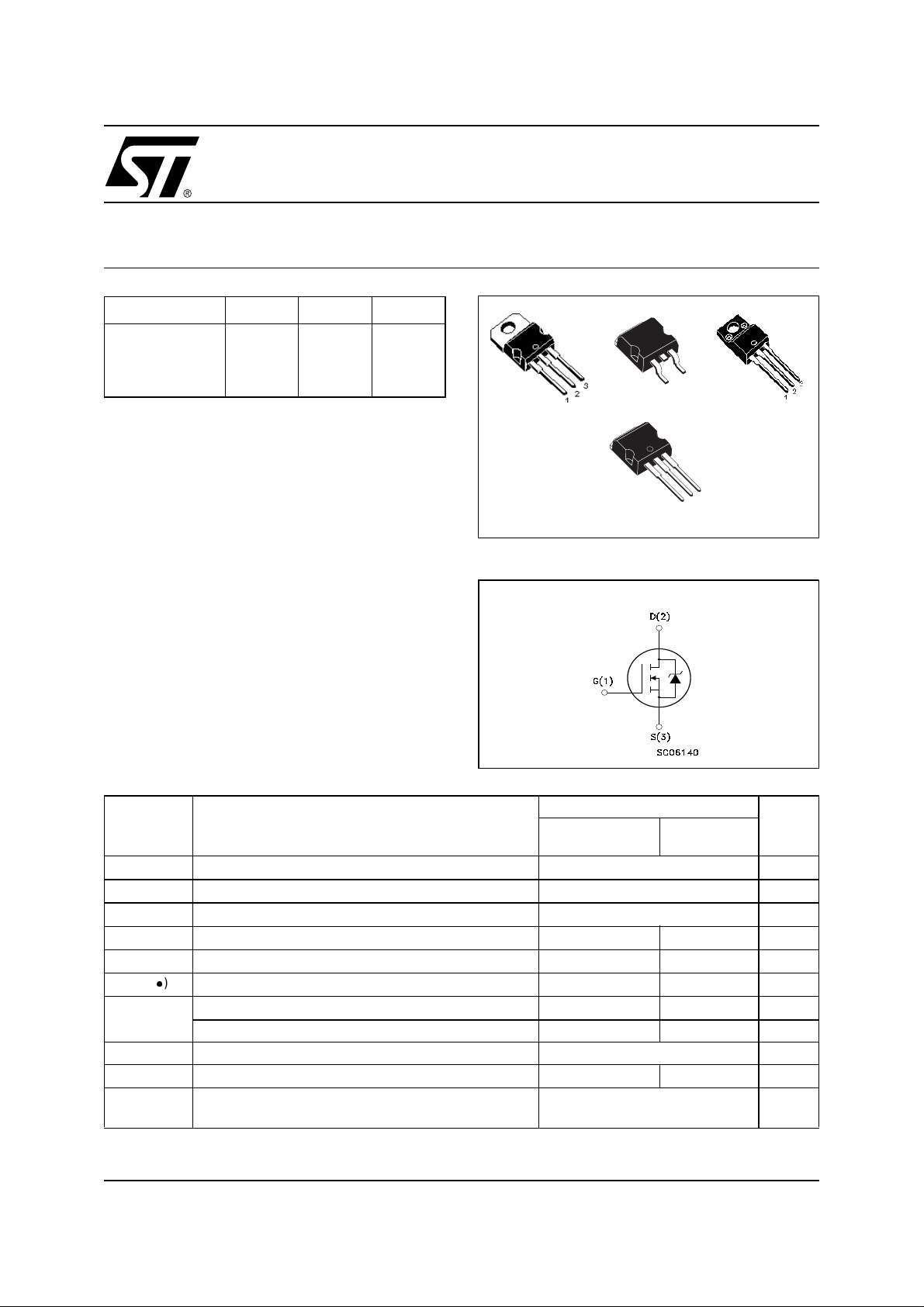
3
1
TO-220
D2PAK
3
2
1
TO-220FP
I2PAK
INTERNAL SCHEM ATIC DIAGRAM
ABSOLUTE MAXIMUM RATINGS
Symbol Parameter Value Unit
STP5NC50
STB5NC50/-1
Drain-source Voltage (VGS=0)
Drain-gate Voltage (RGS=20kΩ)
Gate- source Voltage ±30 V
Drain Current (continuos) at TC= 25°C
Drain Current (continuos) at TC= 100°C
()
Drain Current (pulsed) 22 22 A
Total Dissipation at TC= 25°C
5.5 5.5(*) A
3.5 3.5(*) A
100 35 W
I
V
DM
P
V
DGR
V
I
I
TOT
DS
GS
D
D
Derating Factor 0.8 0.28 W/°C
dv/dt(1) Peak Diode Recovery voltage slope 3.5 V/ns
V
ISO
T
T
stg
(•)Pulse width limited by safe operating area
≤5.5A, di/dt ≤100A/µs, VDD≤ V
(1)I
SD
Insulation Withstand Voltage (DC) - 2500 V
Operating Junction Temperature
j
Storage Temperature
(*)Limited only by maximum temperature allowed
(BR)DSS,Tj≤TJMAX.
-55 to 175
-65 to 175
STP5NC50FP
500 V
500 V
°C
°C
1/12December 2002
STP5NC50 - ST P5NC 50FP - STB5N C50 - STB5NC50-1
THERMAL DATA
TO-220
2
D
PAK
2
PAK
I
Rthj-case Thermal Resistance Junction-case Max 1.25 3.57 °C/W
Rthj-amb Thermal Resistance Junction-ambient Max 62.5 °C/W
T
Maximum Lead Temperature For Soldering Purpose 300 °C
l
AVALANCHE CHARACTERISTICS
Symbol Parameter Max Value Unit
I
AR
E
AS
Avalanche Current, Repetitive or Not-Repetitive
(pulse width limited by T
max)
j
Single Pulse Avalanche Energy
(starting T
= 25 °C, ID=IAR,VDD=50V)
j
ELECTRICAL CHARACTERISTICS (TCASE = 25 °C UNLESS OTHE RWIS E SPECIFIED)
OFF
Symbol Parameter Test Conditions Min. Typ. Max. Unit
V
(BR)DSS
I
DSS
I
GSS
Drain-source
Breakdown Voltage
Zero Gate Voltage
Drain Current (V
GS
Gate-body Leakage
Current (V
DS
=0)
=0)
ID= 250µA, VGS= 0 500 V
V
= Max Rating
DS
= Max Rating, TC= 125 °C
V
DS
V
= ±30V ±100 nA
GS
TO-220FP
5.5 A
280 mJ
1µA
50 µA
(1)
ON
Symbol Parameter Test Conditions Min. Typ. Max. Unit
V
GS(th)
R
DS(on)
Gate Threshold Voltage
Static Drain-source On
V
DS=VGS,ID
VGS=10V,ID=2A
= 250µA
234V
1.3 1.5 Ω
Resistance
DYNAMIC
Symbol Parameter Test Conditions Min. Typ. Max. Unit
(1)
g
fs
C
iss
C
oss
C
rss
Forward Transconductance VDS>I
Input Capacitance
Output Capacitance 80 pF
Reverse Transfer
Capacitance
D(on)xRDS(on)max,
ID= 2.5A
V
=25V,f=1MHz,VGS=0
DS
4S
480 pF
11.5 pF
2/12
STP5NC50 - STP5NC50FP - STB5NC50 - STB5NC50-1
ELECTRICAL CHARACTERISTICS
(CONTINUED)
SWITCHING ON
Symbol Parameter Test Conditions Min. Typ. Max. Unit
V
t
d(on)
t
r
Q
Q
gs
Q
gd
Turn-on Delay Time
Rise Time
Total Gate Charge
g
Gate-Source Charge 3 nC
Gate-Drain Charge 9 nC
SWITCHING OFF
Symbol Parameter Test Conditions Min. Typ. Max. Unit
t
r(Voff)
t
t
f
c
Off-voltage Rise Time
Fall Time 14 ns
Cross-over Time 20 ns
SOURCE DR AIN DIODE
Symbol Parameter Test Conditions Min. Typ. Max. Unit
I
SD
I
SDM
V
SD
t
rr
Q
rr
I
RRM
Note: 1. Pulsed:Pulseduration=300µs,dutycycle1.5%.
2. Pulse width limited by safeoperating area.
Source-drain Current 5.5 A
(2)
Source-drain Current (pulsed) 22 A
(1)
Forward On Voltage
Reverse Recovery Time
Reverse Recovery Charge 1.6 µC
Reverse Recovery Current 9 A
=250V,ID= 2.5A
DD
R
= 4.7Ω VGS=10V
G
(see test circuit, Figure 3)
V
=400V,ID= 5.5A,
DD
=10V
V
GS
V
= 400V, ID= 5.5A,
DD
RG=4.7Ω, VGS= 10V
(see test circuit, Figure 5)
ISD= 5.5A, VGS=0
I
= 5.5A, di/dt = 100A/µs,
SD
VDD=100V,Tj=150°C
(see test circuit, Figure 5)
14 ns
15 ns
17.5 24.5 nC
12 ns
1.6 V
360 ns
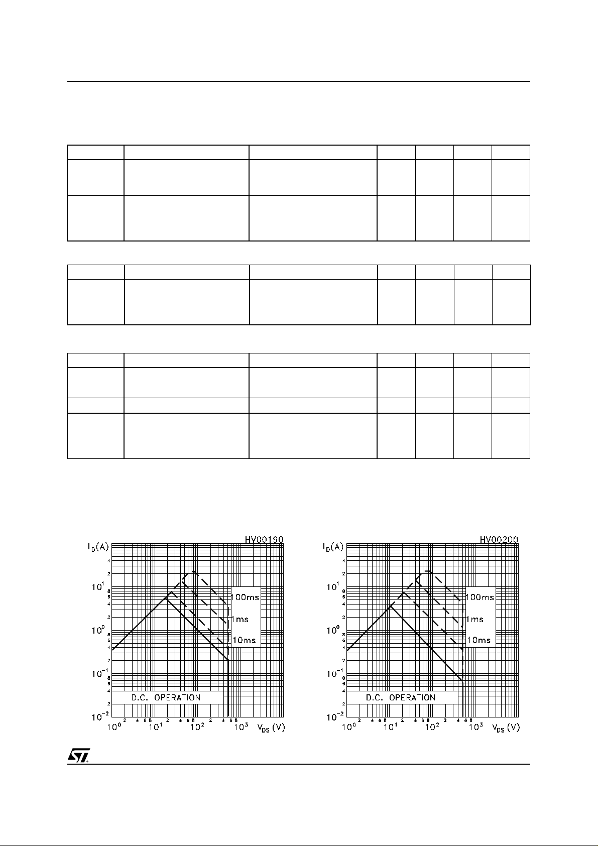
Safe Operating Area for TO-220FPSafe Operating Area for TO-220/D2PAK/I2PAK
3/12
STP5NC50 - ST P5NC 50FP - STB5N C50 - STB5NC50-1
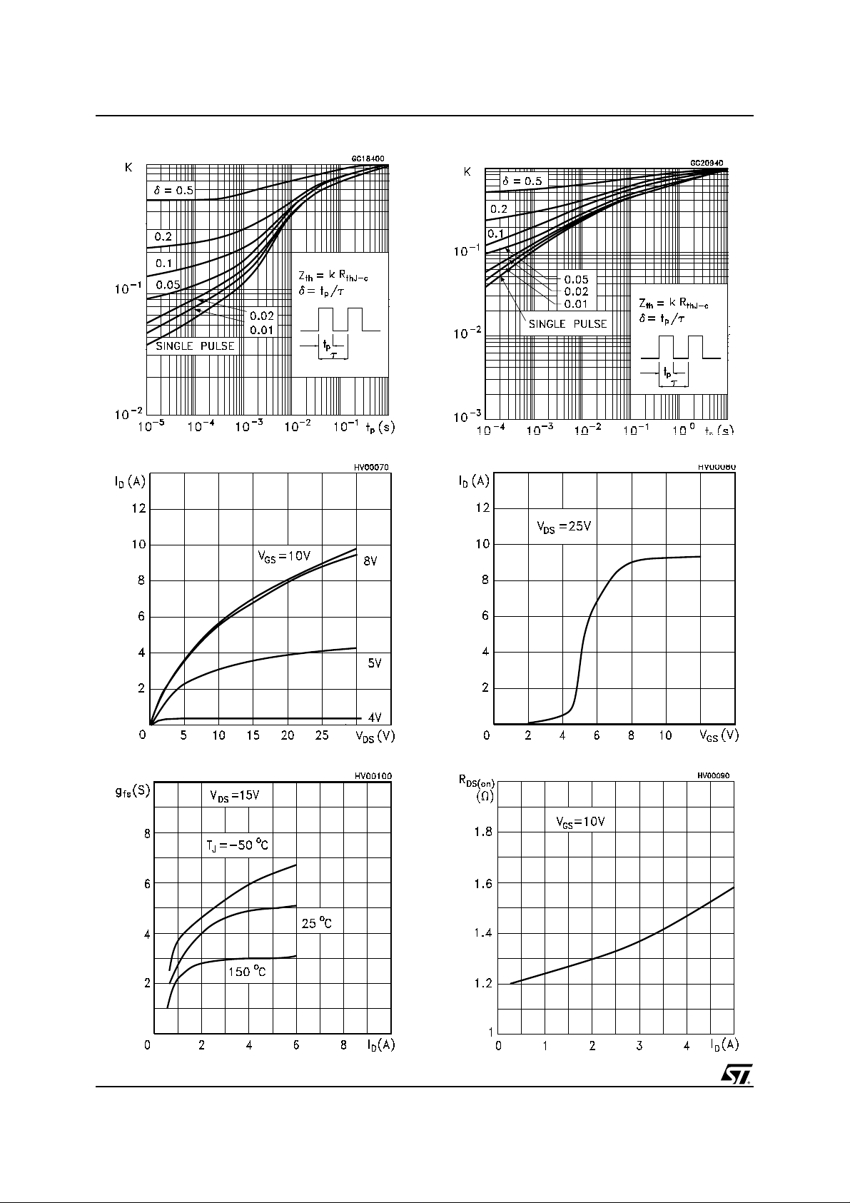
Thermal Impedence for TO-220/D2PAK/I2PAK
Output Characteristics
Thermal Impedence for TO-220FP
Transfer Characteristics
Transconductance Static D rain-source On Resistance
4/12
 Loading...